

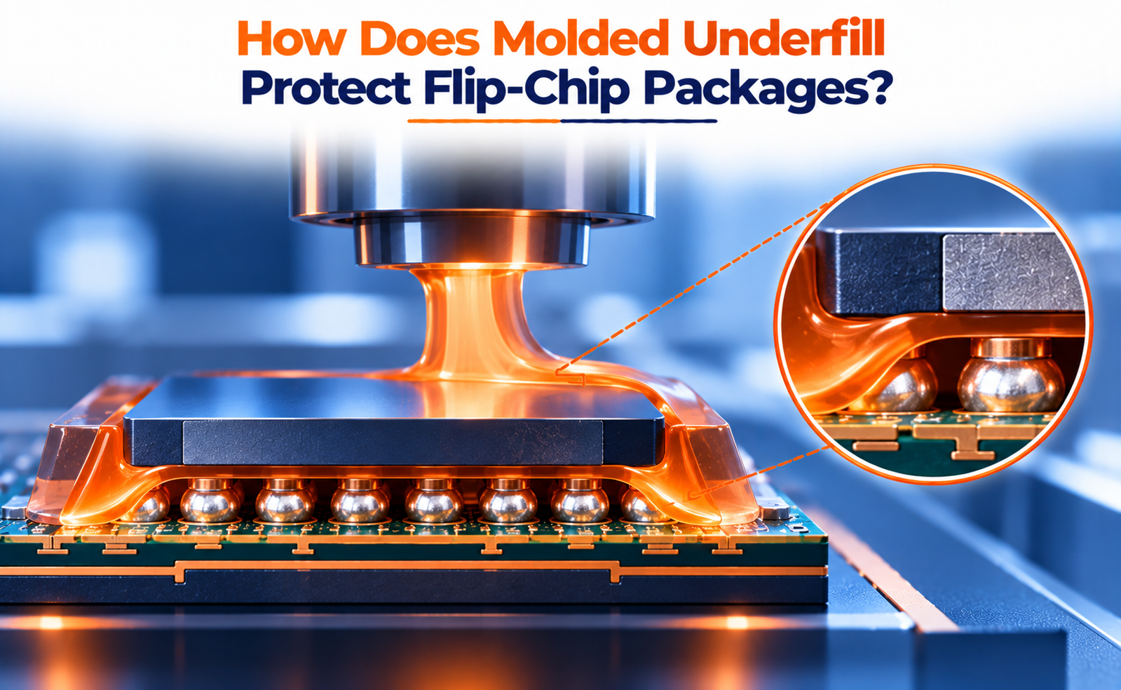
Molded underfill (MUF) is an important packaging technology that improves the mechanical reliability of flip-chip semiconductor devices. It encapsulates the tiny solder bumps or interconnects between a silicon die and its package substrate, helping distribute mechanical stress, protect against environmental damage, and support reliable electrical connections. As advanced chips become more powerful and package interconnects become denser, molded underfill plays an increasingly important role in semiconductor packaging.
What Is Molded Underfill in Flip-Chip Packaging?
Molded underfill (MUF) is an encapsulation technique that combines underfill and package molding into a single integrated process. A specialized epoxy molding compound fills the narrow gap between the silicon die and the substrate while also forming a protective layer around the die.
In flip-chip packaging, the active surface of the chip faces the substrate. Tiny solder bumps or copper-based interconnects establish electrical connections between the two. However, these interconnects are exposed to mechanical stress caused by differences in the thermal expansion of silicon, solder, and substrate materials.
MUF surrounds these interconnects with a mechanically supportive material, helping distribute stress and stabilize the package.
Its main functions include:
- Supporting solder bumps and other interconnect structures.
- Reducing localized thermomechanical stress.
- Protecting the die and interconnect region against mechanical damage.
- Improving package robustness during handling and operation.
- Combining underfilling and encapsulation to simplify manufacturing.
How Does Molded Underfill Protect Solder Bumps?
Solder bumps provide both electrical connectivity and mechanical attachment between a flip-chip die and its package substrate. During operation, the package experiences temperature changes, vibration, and mechanical loading that can stress these connections.
One major source of stress is the coefficient of thermal expansion (CTE) mismatch between silicon and the substrate. These materials expand and contract by different amounts as temperature changes, creating shear stress in the solder bumps.
MUF helps by distributing part of this stress through the surrounding encapsulant instead of allowing the solder joints to absorb it alone.
This support can help reduce solder fatigue and the likelihood of cracks developing during repeated thermal cycling. It can also help maintain stable connections under mechanical loading.
However, the benefit depends on the material properties and package design. An unsuitable modulus, excessive residual stress, or poor adhesion can transfer stress to other locations, including the die and material interfaces.
What Materials Are Used in Molded Underfill?
MUF materials are typically based on epoxy molding compounds (EMCs) engineered to flow into narrow gaps while providing the required mechanical and thermal properties after curing.
These compounds generally contain an epoxy resin system, curing agents, silica fillers, and additives that control processing and final performance.
Important material properties include:
Coefficient of thermal expansion: A lower, well-matched CTE can help reduce thermally induced deformation and stress.
Elastic modulus: The material must provide sufficient mechanical support without creating excessive stress concentrations.
Flowability: The compound must flow around dense bump arrays and fill the space beneath the die without trapping air.
Filler size and distribution: Fine, well-controlled fillers help the compound enter narrow gaps while contributing to dimensional stability and reduced thermal expansion.
Adhesion: Strong adhesion to the die, substrate, and surrounding materials helps limit delamination.
Moisture resistance and thermal stability: The cured compound must withstand the intended operating environment and package processing conditions.
Why Is Molded Underfill Important for Advanced Semiconductor Packaging?
As semiconductor packages integrate more functions into smaller spaces, interconnect density and thermal demands continue to increase. MUF is attractive for applications where manufacturing throughput, compact packaging, and mechanical reliability are important.
Potential applications include mobile processors, consumer electronics, high-performance computing packages, system-in-package designs, and selected advanced packaging architectures.
Its integrated process can help reduce manufacturing complexity and support high-volume production. The cured encapsulant also provides mechanical reinforcement around the die and interconnect region.
However, MUF is not automatically the best option for every package. Fine-pitch interconnects, very small die-to-substrate gaps, large die sizes, and stringent warpage limits may require specialized materials and tightly controlled process conditions. Some designs may favor conventional capillary underfill or other encapsulation approaches depending on reliability and integration requirements.
Conclusion
Molded underfill protects flip-chip packages by reinforcing the interconnect region, redistributing thermomechanical stress, and encapsulating the die within a protective molding compound. Its ability to combine underfilling and molding in an integrated process can also improve manufacturing efficiency.
Reliable MUF implementation depends on material selection, complete gap filling, strong interfacial adhesion, and careful control of void formation and package warpage.
As semiconductor packaging advances toward higher interconnect density and greater functional integration, molded underfill remains an important technology for supporting durable electrical connections and dependable package performance.
Share your question in comments or talk to our mentor team for batch guidance.
Ask the Admin Team
Drop your basic question in comments: eligibility, prerequisites, tools, fee range, and placement support.
Our team reviews and responds regularly.