

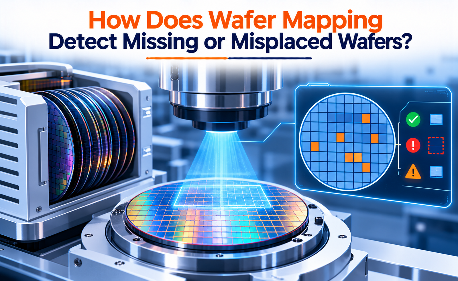
Semiconductor manufacturing depends on precise wafer handling at every stage of production. Silicon wafers move between storage carriers, robotic handling systems, inspection equipment, and process tools. If a wafer is missing, tilted, or placed in the wrong slot, it can interrupt production and potentially damage valuable wafers or equipment.
Wafer mapping is an automated detection process that identifies the occupancy and position of wafers inside a carrier, such as a cassette or Front Opening Unified Pod (FOUP). By using optical sensors, laser-based detection, imaging systems, and equipment-control software, wafer mapping verifies whether wafers are present and correctly positioned before handling or processing begins.
What Is Wafer Mapping in Semiconductor Manufacturing?
Wafer mapping is the process of determining the status of individual wafer slots within a storage carrier. Each slot is checked to establish whether it is occupied, empty, or associated with an abnormal wafer position.
A wafer map represents this information as a slot-by-slot record that automated material handling systems and process tools can use.
For example, a carrier may contain 25 wafer slots, but only 23 wafers may be loaded. The mapping system identifies the occupied and empty slots instead of assuming that every slot contains a wafer.
Wafer mapping can help detect several abnormal conditions:
- Missing wafer: An expected slot is empty.
- Cross-slotted wafer: A wafer is inserted incorrectly and may overlap or interfere with a neighboring slot.
- Double wafer: Two wafers occupy the same slot or are positioned too closely together.
- Tilted wafer: A wafer is not resting in its intended horizontal position.
- Protruding wafer: A wafer extends beyond its expected position inside the carrier.
- Broken or displaced wafer: Abnormal sensor readings or imaging patterns indicate a possible handling problem.
Which Sensors Are Used to Detect Missing or Misplaced Wafers?
Wafer mapping systems use different sensing technologies depending on the carrier design, wafer material, thickness, reflectivity, and required detection accuracy.
Optical beam sensors
An optical sensor sends a light beam across a wafer slot. When a wafer interrupts the beam, the sensor detects a change in the received light signal. As the sensor scans successive slot positions, the system determines which slots contain wafers.
Laser displacement sensors
Laser sensors measure reflected light or the distance to a target surface. Changes in the measured position can indicate whether a wafer is present, protruding, or tilted. Comparing measurements from different sensor positions can provide additional information about wafer alignment.
Imaging-based mapping systems
Camera-based systems capture images of wafer edges and slot regions. Image-processing software analyzes these images to determine wafer presence and identify abnormal loading patterns. Some systems can inspect wafers through suitable carrier windows without opening the carrier.
Specialized sensors for thin or transparent wafers
Certain wafer materials, coatings, and surface finishes can make conventional optical detection difficult. Specialized mapping sensors are designed to handle variations in reflectivity and wafer properties, improving detection reliability.
Why Is Wafer Mapping Important for Yield and Equipment Safety?
Wafer mapping contributes to both manufacturing efficiency and equipment protection.
Prevents wafer collisions: Confirming slot occupancy helps prevent a robot from inserting a wafer into an already occupied slot or retrieving one from an empty slot.
Reduces wafer breakage: Detecting tilted, cross-slotted, or protruding wafers can prevent handling operations that might cause contact or mechanical damage.
Protects production equipment: Abnormal wafer positions can be identified before they interfere with robot blades, carrier mechanisms, or process-tool components.
Improves traceability: Slot-level information helps equipment maintain an accurate record of wafer locations and loading conditions.
Reduces unnecessary downtime: Early detection allows operators to investigate carrier-loading problems before they interrupt a longer production sequence.
Supports automated manufacturing: Reliable wafer-position information helps coordinate robotic transfers and material movement across multiple process tools.
Because semiconductor wafers may contain substantial processing value, preventing a single handling incident can be important to overall manufacturing economics.
What Challenges Affect Wafer Mapping Accuracy?
Although wafer mapping is a well-established automation function, several factors can affect its reliability.
Wafer material and reflectivity: Transparent wafers, dark coatings, and unusual surface finishes can change the amount of light returned to an optical sensor.
Sensor calibration: Incorrect sensor alignment or slot-position settings can cause occupied slots to be classified incorrectly.
Carrier variation: Different cassette and FOUP designs may require different sensing positions, calibration parameters, or image-processing configurations.
Mechanical tolerances: Carrier placement, slot geometry, and wafer-edge positioning can affect measurement repeatability.
Contamination and optical interference: Dust, residue, reflections, and obstructed optical paths may affect sensor signals.
Complex loading conditions: A simple presence check may not be sufficient to distinguish between a correctly placed wafer and a wafer that is tilted, cross-slotted, or overlapping another wafer.
To address these challenges, manufacturers combine appropriate sensor selection, carrier-specific calibration, signal validation, preventive maintenance, and equipment interlocks. When a mapping result is uncertain, the equipment can be configured to stop or request additional verification rather than proceeding with an unsafe transfer.
Conclusion
Wafer mapping is an essential safeguard in semiconductor manufacturing automation. By scanning wafer slots and analyzing sensor measurements, it helps identify missing wafers, incorrect placement, tilting, cross-slotting, and other abnormal loading conditions.
Optical sensors, laser-based systems, imaging technologies, and control software work together to create a reliable representation of wafer positions inside a cassette or FOUP. This information helps robotic systems make safer transfer decisions, reduces handling-related defects, and supports uninterrupted manufacturing.
As semiconductor production becomes increasingly automated, accurate wafer mapping remains a key requirement for protecting wafers, improving equipment reliability, and maintaining high manufacturing yield.
Share your question in comments or talk to our mentor team for batch guidance.
Ask the Admin Team
Drop your basic question in comments: eligibility, prerequisites, tools, fee range, and placement support.
Our team reviews and responds regularly.