

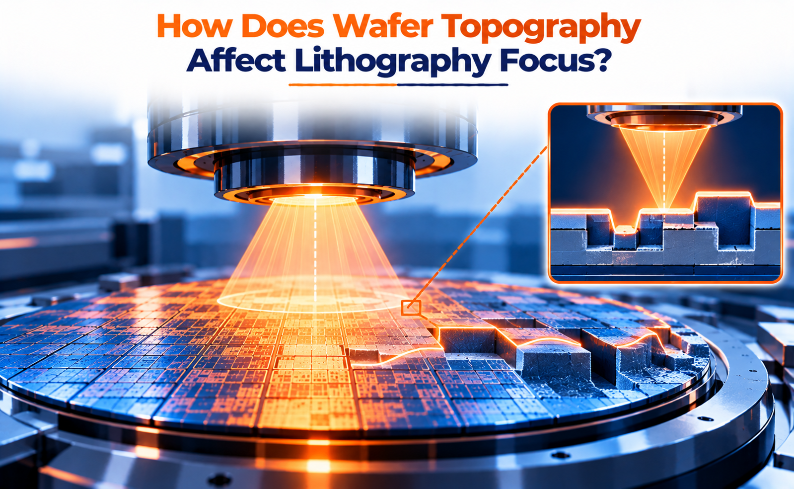
Wafer topography plays a critical role in semiconductor lithography because the wafer surface is rarely perfectly flat. Variations in height caused by deposited films, etched structures, metal interconnects, and previous manufacturing steps can affect how accurately a lithography system focuses its image on the photoresist.
As semiconductor features become smaller, even minor surface-height variations can reduce pattern quality, distort critical dimensions, and increase defect risk. Understanding wafer topography is therefore essential for maintaining focus accuracy and reliable pattern transfer in advanced chip manufacturing.
What Is Wafer Topography in Semiconductor Manufacturing?
Wafer topography refers to the height variations and surface features present across a semiconductor wafer. Although silicon wafers are manufactured to be highly flat, subsequent fabrication steps create raised and recessed regions on their surfaces.
Common sources of wafer topography include:
- Deposition: Different film thicknesses create variations in surface height.
- Etching: Trenches, contact holes, and recessed structures form depressions.
- Metal interconnects: Conductive lines and vias introduce local height variations.
- Chemical Mechanical Planarization (CMP): Dishing and erosion can leave residual surface irregularities.
- Pattern-density variations: Regions containing dense structures may polish or deposit differently from less dense regions.
These variations can occur across the entire wafer, within an individual exposure field, or over very small regions of a chip.
Why Does Lithography Require Precise Focus?
Photolithography transfers circuit patterns onto a light-sensitive material called photoresist. A projection optical system focuses the mask pattern onto the resist-coated wafer, creating an image that is subsequently developed.
The quality of this image depends on several factors, including exposure wavelength, numerical aperture, optical aberrations, and focus position.
An important parameter is the depth of focus (DOF), which describes the range of focus positions over which the projected image maintains acceptable quality.
When the wafer surface lies within the appropriate focus range, the system can produce well-defined patterns. When portions of the resist surface move outside this range, the image may become blurred and its dimensions may change.
Modern lithography systems use autofocus and wafer-leveling mechanisms to compensate for wafer shape and height variations. However, these systems have finite measurement accuracy and correction capabilities. Rapid local height changes and differences between the measured surface and the actual resist surface can still introduce focus errors.
How Does Wafer Topography Cause Focus Errors?
Wafer topography affects lithography focus by changing the vertical distance between the photoresist surface and the optical system’s intended focal plane.
Consider a wafer containing a raised metal region beside a recessed dielectric region. Even when both regions are exposed using the same nominal focus setting, their resist surfaces may sit at different heights.
This can produce several focus-related effects.
Local defocus: Raised regions may be closer to the optical system than expected, while recessed regions may be farther away. If the difference exceeds the available focus tolerance, image quality can deteriorate.
Pattern-width variation: Defocus changes the projected image and the resist’s response to exposure. This can cause critical dimensions (CDs) to vary across different regions of the wafer.
Line-edge roughness: Changes in image contrast and exposure conditions can produce less consistent pattern edges.
Contact-hole and via distortion: Small openings may become larger, smaller, or less clearly defined, potentially affecting later etching and electrical connectivity.
Focus-offset variation: Different pattern densities and underlying structures can alter autofocus measurements or shift the optimum exposure focus.
How Does Wafer Topography Affect Photoresist and Critical Dimensions?
Wafer topography can affect lithography both through focus variation and through changes in photoresist coating.
During spin coating, liquid photoresist spreads across the wafer and forms a film. Surface grooves, trenches, and raised features can influence local film thickness, particularly on highly structured surfaces.
Nonuniform resist thickness can change the optical and chemical conditions experienced during exposure and development.
For example, a thicker resist region may respond differently from a thinner region because light absorption, the effective resist profile, and development behavior vary with the local film thickness.
The resulting defects may include:
- Critical dimension nonuniformity: Identical features print at different widths.
- Incomplete pattern formation: Small openings or narrow lines fail to develop as intended.
- Pattern distortion: Feature profiles vary with local focus and resist conditions.
- Overlay errors: Changes in wafer shape and process alignment can complicate the placement of successive layers.
- Reduced process window: Fewer combinations of focus and exposure dose produce acceptable patterns across the wafer.
How Do Semiconductor Manufacturers Control Topography-Related Focus Errors?
Manufacturers use several complementary techniques to control wafer topography and improve lithography performance.
Chemical Mechanical Planarization (CMP)
CMP removes excess material and smooths deposited layers, reducing height differences before subsequent lithography steps. Proper control of dishing, erosion, and polishing uniformity helps maintain a more consistent surface.
Wafer leveling and autofocus
Lithography scanners measure wafer height at selected locations and adjust the wafer stage or focus settings during exposure. These corrections help compensate for wafer bow, tilt, and gradual height variations.
Topography measurement and mapping
Metrology tools measure surface-height variations and generate topography maps. These maps can help identify regions likely to experience focus problems and guide process adjustments.
Resist coating optimization
Appropriate coating conditions and resist formulations help maintain more uniform film thickness over structured surfaces. Spray coating or other specialized methods may be useful for wafers with particularly deep features.
Topography-aware computational correction
Process simulations and layout-aware methods can predict focus variations associated with underlying structures. This information can be used to improve optical proximity correction (OPC), exposure settings, and process integration.
Process integration and pattern-density control
Layout design, dummy-fill structures, deposition uniformity, and CMP optimization can work together to reduce surface-height differences before the next lithography operation.
Why Is Topography Control Critical for Advanced Nodes?
As semiconductor technology advances, manufacturers must print smaller features while maintaining increasingly strict requirements for critical dimensions, overlay, and defectivity.
At the same time, advanced chips contain complex multilayer interconnect structures that can create substantial local differences in pattern density and surface height.
This creates several challenges:
Smaller focus margin: Advanced imaging systems require precise control of the wafer-to-focus relationship. Higher numerical aperture improves resolution but generally makes depth-of-focus control more demanding.
Complex three-dimensional structures: Dense interconnects, high-aspect-ratio features, and repeated deposition and etching steps create challenging surface profiles.
Cumulative process variation: Small errors from deposition, CMP, coating, and focus measurement can combine to produce larger downstream patterning errors.
Increasing yield sensitivity: A focus-related defect in a critical contact, via, or transistor feature can affect device performance or electrical connectivity.
Greater need for integrated process control: Topography information must increasingly be considered alongside lithography settings, resist behavior, design geometry, and upstream process data.
Conclusion
Wafer topography affects lithography focus by changing the height and shape of the photoresist surface relative to the optical system’s focal plane. Variations introduced by deposition, etching, metal patterning, and CMP can cause local defocus, critical-dimension variation, and pattern distortion.
Semiconductor manufacturers address these challenges through planarization, accurate wafer mapping, autofocus and leveling, resist-coating optimization, and topography-aware computational correction.
As chip features continue to shrink, precise control of surface height becomes increasingly important for maintaining imaging quality, improving manufacturing yield, and enabling reliable fabrication of advanced semiconductor devices.
Share your question in comments or talk to our mentor team for batch guidance.
Ask the Admin Team
Drop your basic question in comments: eligibility, prerequisites, tools, fee range, and placement support.
Our team reviews and responds regularly.