Modern semiconductor chips are expected to deliver high performance while consuming minimal power and occupying less silicon area. Achieving the right balance between Performance, Power, and Area (PPA) is one of the most important goals in VLSI design. Every design decision, from architecture to physical implementation, impacts these three factors.
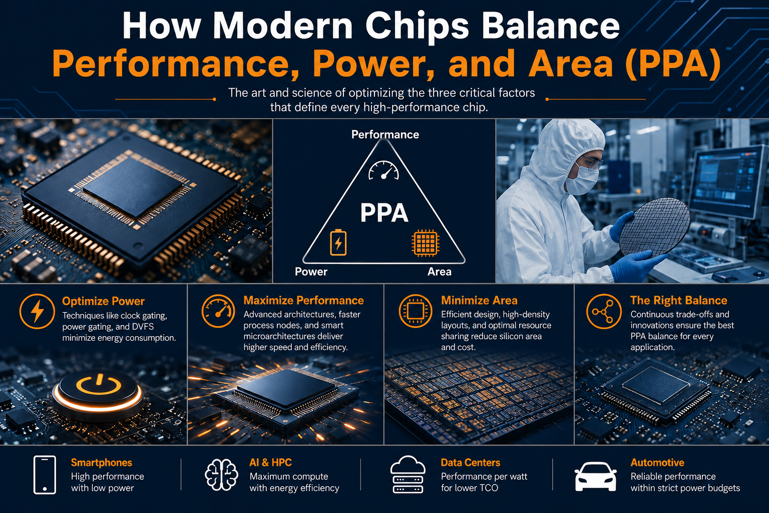
Understanding the PPA Triangle
Performance
Performance determines how fast a chip can execute tasks. Higher clock speeds, improved architectures, and larger caches generally increase performance.
Power
Power consumption affects battery life, thermal management, and operating costs. It includes both dynamic power (switching activity) and leakage power.
Area
Area refers to the amount of silicon used by the design. Smaller chip area reduces manufacturing costs and improves yield.
Since these factors are interconnected, improving one often impacts the others, making PPA optimization a continuous trade-off process.
Why PPA Matters in Modern Chip Design
PPA optimization is critical across various applications:
- Smartphones: Require high performance with long battery life.
- AI Accelerators: Need maximum computational power with energy efficiency.
- Data Centers: Focus on performance per watt to reduce operational costs.
- Automotive Electronics: Demand reliable performance within strict power budgets.
A well-balanced PPA strategy ensures competitive and cost-effective products.
Key Techniques Used to Optimize PPA
Clock Gating
Disables clocks to inactive circuits, reducing dynamic power consumption.
Power Gating
Turns off unused functional blocks to minimize leakage power.
Dynamic Voltage and Frequency Scaling (DVFS)
Adjusts voltage and frequency based on workload requirements to save energy.
Multi-Vt Optimization
Uses different transistor threshold voltages to balance speed and leakage power.
These techniques are widely adopted in modern SoC designs.
The Role of Advanced Process Nodes
Technology scaling has significantly improved PPA over the years.
Benefits of advanced nodes such as 7nm, 5nm, and 3nm include:
- Higher transistor density
- Improved performance
- Lower power consumption
- Better area efficiency
Smaller transistors allow designers to integrate more functionality within the same silicon footprint.
PPA Optimization During Physical Design
Physical design plays a major role in achieving target PPA.
Key optimization areas include:
- Placement optimization
- Routing efficiency
- Clock Tree Synthesis (CTS)
- Timing closure
- Congestion reduction
A well-optimized layout improves performance while minimizing power and area overhead.
Conclusion
Balancing Performance, Power, and Area (PPA) is at the heart of modern chip design. Engineers continuously optimize these factors using advanced architectures, low-power techniques, process technologies, and physical design methodologies. As semiconductor complexity continues to grow, achieving the right PPA balance remains essential for delivering efficient, high-performance, and cost-effective chips.
Share your question in comments or talk to our mentor team for batch guidance.
Ask the Admin Team
Drop your basic question in comments: eligibility, prerequisites, tools, fee range, and placement support.
Our team reviews and responds regularly.
