Semiconductor manufacturing relies on highly precise material removal processes to create the intricate structures found in modern integrated circuits. As device architectures become increasingly complex, manufacturers use different etching techniques depending on the desired feature geometry and application.
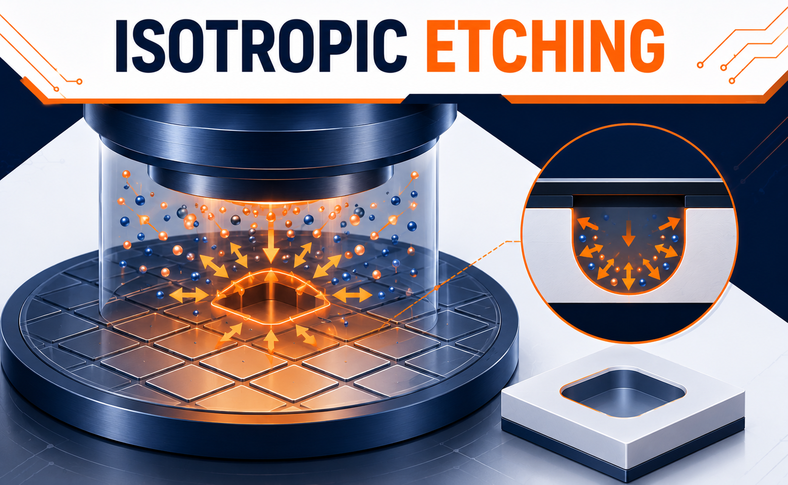
Isotropic Etching is one of the most fundamental etching methods used in semiconductor fabrication. Unlike directional etching techniques, isotropic etching removes material uniformly in all directions, making it ideal for specific fabrication processes that require smooth, rounded profiles or selective material removal. Although advanced technologies often rely on anisotropic etching for nanoscale features, isotropic etching continues to play a critical role in wafer processing, MEMS fabrication, and semiconductor manufacturing.
What is Isotropic Etching?
Isotropic Etching is a material removal process in which the etching rate is nearly equal in every direction. As the etchant attacks the exposed material uniformly, it removes material both vertically and laterally, resulting in rounded or curved feature profiles.
Depending on the manufacturing requirement, isotropic etching can be performed using:
- Wet chemical etching
- Dry plasma-based isotropic etching
- Vapor-phase etching
This uniform material removal makes isotropic etching highly effective for applications where directional precision is not the primary requirement.
Why Isotropic Etching is Important in Semiconductor Manufacturing
Although many advanced transistor structures require highly directional etching, isotropic etching remains an essential process for numerous semiconductor applications.
Its importance includes:
- Uniform material removal
- Smooth surface formation
- High selectivity for specific materials
- Simplified process control
- Excellent compatibility with sacrificial layer removal
- Reduced mechanical damage compared to aggressive physical etching methods
Applications of Isotropic Etching
Isotropic etching is widely used across various semiconductor fabrication processes.
Silicon Wafer Processing
Removes unwanted material during wafer preparation and device fabrication.
MEMS Manufacturing
Creates suspended microstructures, cavities, and release layers for sensors, accelerometers, gyroscopes, and micro-actuators.
Sacrificial Layer Removal
Eliminates temporary materials used during complex semiconductor fabrication without damaging surrounding structures.
Advanced Packaging
Supports cavity formation and selective material removal for advanced semiconductor package manufacturing.
Surface Cleaning and Preparation
Removes residual materials and prepares wafer surfaces before subsequent deposition or fabrication processes.
Advantages
- Uniform material removal
- Smooth etched surfaces
- High process simplicity
- Cost-effective manufacturing
- Suitable for complex cavity formation
- Excellent for sacrificial layer release
- Compatible with various semiconductor materials
The Future of Isotropic Etching
As semiconductor manufacturing evolves, isotropic etching continues to improve through innovations in chemistry and process control.
Emerging developments include:
- Advanced plasma-based isotropic etching
- Greater selectivity for next-generation materials
- Improved process uniformity across large wafers
- Integration with Atomic Layer Etching (ALE) workflows
- Enhanced MEMS fabrication techniques
- AI-assisted process monitoring and optimization
- Sustainable chemical formulations with reduced environmental impact
Conclusion
Isotropic Etching is a fundamental semiconductor fabrication technique that provides uniform material removal across all directions. While it differs from anisotropic etching in profile characteristics, its ability to create smooth surfaces, release sacrificial layers, and fabricate complex microstructures makes it indispensable in modern semiconductor manufacturing.
Share your question in comments or talk to our mentor team for batch guidance.
Ask the Admin Team
Drop your basic question in comments: eligibility, prerequisites, tools, fee range, and placement support.
Our team reviews and responds regularly.