

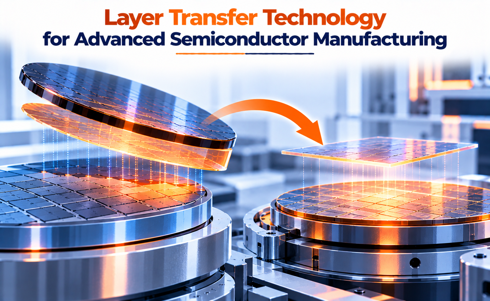
As semiconductor devices become smaller, faster, and more complex, manufacturers are exploring new ways to integrate high-performance materials into advanced chip architectures. Conventional epitaxial growth and bulk-wafer processing can face limitations when different semiconductor materials have mismatched crystal structures, thermal expansion coefficients, or processing requirements.
Layer transfer technology offers an alternative by enabling a thin semiconductor film or functional device layer to be moved from its original substrate to a different receiving substrate. This approach supports heterogeneous integration, engineered substrates, advanced optoelectronics, and next-generation semiconductor devices.
By separating the material-growth process from the final device-integration platform, layer transfer provides greater flexibility in selecting materials and designing semiconductor structures.
What Is Layer Transfer Technology?
Layer transfer is a semiconductor manufacturing technique in which a thin functional layer is separated from a donor substrate and transferred onto a receiving substrate.
The donor substrate is the original wafer on which the layer is grown or prepared. The receiving substrate, sometimes called the handle wafer, is the platform onto which the transferred layer is integrated.
Depending on the technology, the transferred layer may be a thin single-crystal silicon film, a compound semiconductor, an optical material, or another functional semiconductor layer.
Why Is Layer Transfer Important in Semiconductor Manufacturing?
Advanced semiconductor systems increasingly require combinations of materials that cannot always be integrated efficiently through conventional monolithic fabrication.
For example, silicon is widely used for digital logic, while compound semiconductors can offer attractive properties for high-frequency electronics, light emission, optical detection, and power devices.
Layer transfer provides a pathway for combining these materials on a common platform.
Heterogeneous Integration
Different semiconductor materials can be integrated into one system to combine their complementary electrical, optical, or thermal properties.
Improved Material Selection
A functional layer can be grown or prepared on a suitable donor substrate before being transferred to a different receiving substrate.
Engineered Substrates
Layer transfer can create specialized substrates such as silicon-on-insulator (SOI), where a thin silicon layer is separated from the supporting silicon substrate by a buried insulating layer.
Potential Substrate Reuse
Some transfer methods allow the original donor substrate to be reused after the functional layer is removed, potentially reducing material consumption and cost.
Advanced Device Architectures
Transferred layers can support compact electronic, photonic, sensor, and optoelectronic structures that are difficult to realize using conventional material integration alone.
Major Layer Transfer Techniques
Several techniques are used to transfer semiconductor layers. The appropriate method depends on the material, desired layer thickness, substrate properties, and final application.
Smart Cut and Ion-Cut Technology
Smart Cut-type processes use ion implantation, wafer bonding, and controlled splitting to transfer a thin semiconductor layer onto a receiving substrate.
A weakened region is created inside the donor wafer through implantation. After bonding the donor to the receiving substrate, a suitable thermal or mechanical process separates the wafer along the implanted region.
The transferred surface is then processed as needed to achieve the required thickness and quality.
Wafer Bonding and Thinning
In this approach, the donor wafer is bonded to a receiving substrate. The original substrate is then reduced through grinding, polishing, etching, or a combination of techniques until the desired functional layer remains.
The method is useful when the transferred layer must be supported by a different substrate.
Epitaxial Lift-Off
Epitaxial lift-off uses a selectively removable layer or interface to release a semiconductor film from its growth substrate.
It is particularly relevant to selected compound-semiconductor and optoelectronic applications where preserving the functional layer and potentially recovering the growth substrate are important.
Laser-Assisted Lift-Off
Laser lift-off uses localized laser energy to facilitate separation at a suitable interface. It has been used in selected semiconductor and optoelectronic manufacturing processes, including the transfer of thin films from growth substrates.
The Future of Layer Transfer in Advanced Semiconductor Manufacturing
Layer transfer is expected to remain an important technology as semiconductor systems increasingly combine dissimilar materials and functional layers.
Potential development areas include:
- Higher-quality thin-film transfer
- Lower-defect bonding interfaces
- Improved donor-substrate reuse
- Better control of transferred-layer thickness
- Lower-temperature transfer processes
- Integration of compound semiconductors with silicon
- Advanced electronic-photonic integration
- Micro-LED and display technologies
- Engineered substrates for specialized devices
- Integration of multiple functional layers
The technology is especially relevant to heterogeneous integration, where the objective is to combine complementary material systems without requiring every material to be grown directly on the same substrate.
For example, transferring a compound-semiconductor layer onto a silicon platform can provide a route toward combining optical or high-frequency functions with silicon-based electronics. Engineered substrates can also help address specific device requirements that conventional bulk wafers may not satisfy.
Conclusion
Layer transfer technology expands the possibilities of semiconductor manufacturing by allowing functional material layers to be integrated onto substrates different from those on which they were originally prepared.
Through techniques such as Smart Cut, wafer bonding and thinning, epitaxial lift-off, and laser-assisted separation, manufacturers can develop engineered substrates and heterogeneous structures for advanced electronic, photonic, and optoelectronic applications.
Although interface quality, material damage, thickness uniformity, and manufacturing yield remain important challenges, continued improvements in bonding, separation, and surface finishing are making layer transfer increasingly versatile.
Share your question in comments or talk to our mentor team for batch guidance.
Ask the Admin Team
Drop your basic question in comments: eligibility, prerequisites, tools, fee range, and placement support.
Our team reviews and responds regularly.