

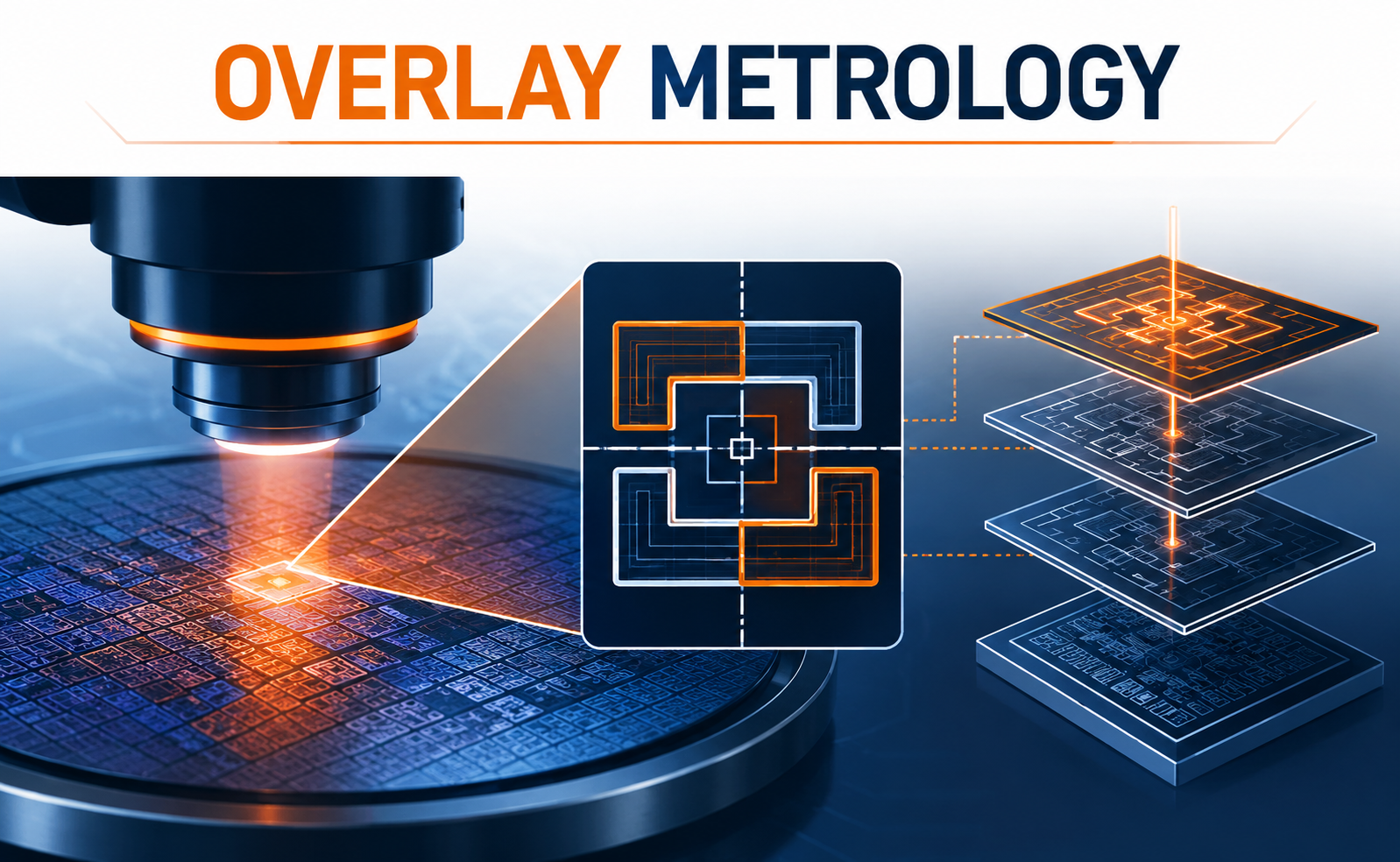
As semiconductor devices continue to shrink, alignment accuracy has become one of the most critical challenges in wafer fabrication. Modern chips are built through dozens of lithography and patterning steps, and every new layer must align precisely with the layers beneath it.
This is where Overlay Metrology plays a crucial role.
Overlay metrology measures the positional difference between patterns created on different wafer layers. By detecting even extremely small alignment errors, it helps semiconductor manufacturers maintain process control, improve yield, and enable increasingly advanced technology nodes.
What Is Overlay Metrology?
Overlay metrology is the measurement of the alignment between two or more patterned layers on a semiconductor wafer.
During fabrication, a wafer passes through multiple lithography steps. Each step creates specific structures that must be positioned accurately relative to previously fabricated layers.
For example:
Layer 1 → Layer 2 → Layer 3 → Layer 4
If Layer 3 shifts slightly relative to Layer 2, electrical connections may no longer land where intended.
Overlay error can occur in several directions, including:
- X-direction error – horizontal displacement
- Y-direction error – vertical displacement
- Rotational error – slight angular misalignment
- Magnification error – differences in pattern scaling
- Wafer-level distortion – non-uniform alignment across the wafer
Overlay metrology quantifies these errors so that manufacturers can identify and correct process problems.
Why Overlay Accuracy Matters
As device dimensions become smaller, the tolerance for alignment errors becomes increasingly tight.
A small overlay error that might have been acceptable at a larger technology node can become a serious problem in advanced semiconductor manufacturing.
Poor overlay control can lead to:
- Misaligned interconnects
- Increased electrical resistance
- Leakage or short circuits
- Defective transistors
- Reduced device performance
- Lower wafer yield
- Increased manufacturing costs
The challenge becomes even greater for technologies involving 3D structures, advanced logic, DRAM, NAND, and heterogeneous integration.
In these applications, multiple layers must work together with extremely high positional accuracy.
Better overlay control → Better pattern alignment → Higher process stability → Higher yield
Overlay Metrology in Process Control
Overlay metrology is not simply a measurement step it is an important component of semiconductor process control.
Manufacturers use overlay data to understand how lithography and wafer-processing steps are behaving.
For example, if overlay errors gradually increase toward the wafer edge, engineers may investigate factors such as:
- Wafer deformation
- Lithography tool behavior
- Stage positioning
- Thermal effects
- Process-induced distortion
- Wafer chucking
- Pattern-related effects
The measurement results can then be fed into process-control systems to adjust subsequent processing.
This creates a continuous feedback loop:
Measure → Analyze → Correct → Re-measure
Such feedback becomes increasingly important as manufacturing tolerances become tighter.
Overlay Metrology Challenges at Advanced Nodes
Advanced semiconductor manufacturing introduces several new challenges for overlay measurement.
Smaller Features
When structures become extremely small, even a very small positional shift can become significant.
Wafer Distortion
Processing steps can introduce wafer-level and local distortions that make alignment more difficult.
3D Device Structures
Modern devices increasingly use complex three-dimensional architectures, making conventional two-dimensional alignment assumptions less sufficient.
Process Variability
Different process steps can introduce local variations, making it important to understand overlay at both global and local levels.
Measurement vs. Production Speed
Manufacturers need extremely accurate measurements without slowing down high-volume manufacturing.
Therefore, modern overlay metrology must balance accuracy, sensitivity, measurement speed, and process integration.
Conclusion
Overlay metrology is one of the foundations of modern semiconductor process control. It transforms microscopic alignment differences into measurable data that engineers can use to optimize lithography, control process variation, and improve wafer yield.
From conventional planar devices to advanced 3D architectures and next-generation integration technologies, precise layer-to-layer alignment will remain essential.
In semiconductor manufacturing, every nanometer matters and overlay metrology helps make sure those nanometers are under control.
Share your question in comments or talk to our mentor team for batch guidance.
Ask the Admin Team
Drop your basic question in comments: eligibility, prerequisites, tools, fee range, and placement support.
Our team reviews and responds regularly.