

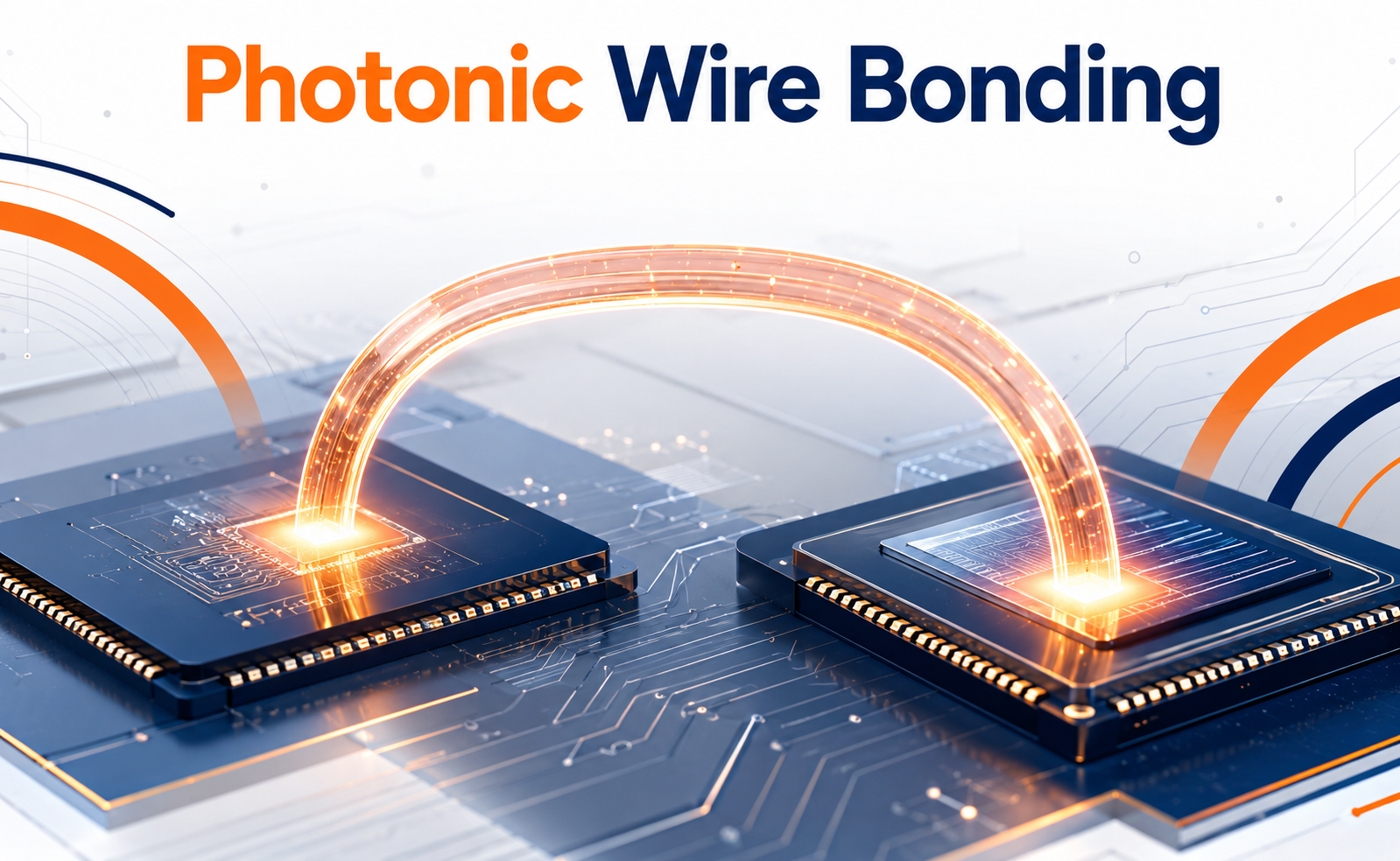
As photonic technologies move toward higher bandwidth, lower latency, and increasingly compact systems, connecting optical components with conventional assembly methods is becoming more challenging. Photonic Wire Bonding (PWB) offers a promising approach by creating precise three-dimensional optical interconnects between photonic components.
Unlike conventional wire bonding used in electronics, photonic wire bonding creates tiny polymer optical waveguides that directly connect optical interfaces. This technology is gaining attention for applications in silicon photonics, optical transceivers, data centers, LiDAR, quantum photonics, and advanced heterogeneous integration.
What Is Photonic Wire Bonding?
Photonic Wire Bonding is an optical packaging technology used to connect photonic chips, optical fibers, lasers, detectors, and other optical components.
The process typically uses two-photon polymerization (2PP), an advanced laser-based 3D printing technique. A photosensitive polymer is selectively cured to form a customized optical waveguide between two optical interfaces.
The resulting structure can compensate for differences in:
- Chip position
- Optical interface height
- Alignment tolerance
- Component geometry
- Packaging architecture
This makes PWB particularly attractive for complex photonic assemblies where conventional planar waveguides may be difficult to implement.
Why Is Photonic Wire Bonding Important?
One of the biggest challenges in photonic packaging is precise optical alignment.
Traditional optical coupling approaches can require extremely accurate placement of components. As photonic systems become smaller and more heterogeneous, achieving this alignment economically becomes increasingly difficult.
PWB changes the approach by allowing the optical connection itself to be fabricated after component placement.
This provides several advantages:
- Three-dimensional routing: Optical connections can move in multiple directions.
- Relaxed placement requirements: The waveguide can compensate for certain component-position variations.
- Direct chip-to-chip connectivity: Different photonic platforms can potentially be interconnected.
- Compact packaging: Complex optical paths can be routed within a small volume.
- Flexible integration: Different components can be connected without requiring identical optical interface layouts.
Applications Across the Photonics Industry
Photonic Wire Bonding has potential across several emerging technology areas.
Data Centers and Optical Communications
High-speed optical systems require compact, low-loss connections between photonic integrated circuits, lasers, detectors, and fiber interfaces. PWB can support dense optical packaging architectures.
Silicon Photonics
Silicon photonics often combines components manufactured using different semiconductor materials and processes. Photonic wire bonds can provide flexible optical connections between these heterogeneous platforms.
LiDAR
Compact optical systems for autonomous vehicles, robotics, and sensing can benefit from precise interconnection between lasers, photonic circuits, and detectors.
Quantum Photonics
Quantum systems can require complex connections between photonic components. The three-dimensional nature of PWB offers opportunities for dense optical integration.
Optical Computing and AI Hardware
As photonic computing architectures develop, scalable optical interconnects could become increasingly important for connecting photonic processing elements.
Conclusion
Photonic Wire Bonding represents a shift from fixed optical assembly toward adaptive three-dimensional optical interconnection. By using precision 3D fabrication to create customized waveguides between photonic components, it can address some of the alignment and integration challenges associated with increasingly complex photonic systems.
As silicon photonics, optical computing, high-speed communications, LiDAR, and quantum technologies continue to evolve, advanced photonic packaging will become just as important as the photonic devices themselves.
Photonic Wire Bonding could play an important role in building the next generation of compact, scalable, and heterogeneous photonic systems.
Share your question in comments or talk to our mentor team for batch guidance.
Ask the Admin Team
Drop your basic question in comments: eligibility, prerequisites, tools, fee range, and placement support.
Our team reviews and responds regularly.