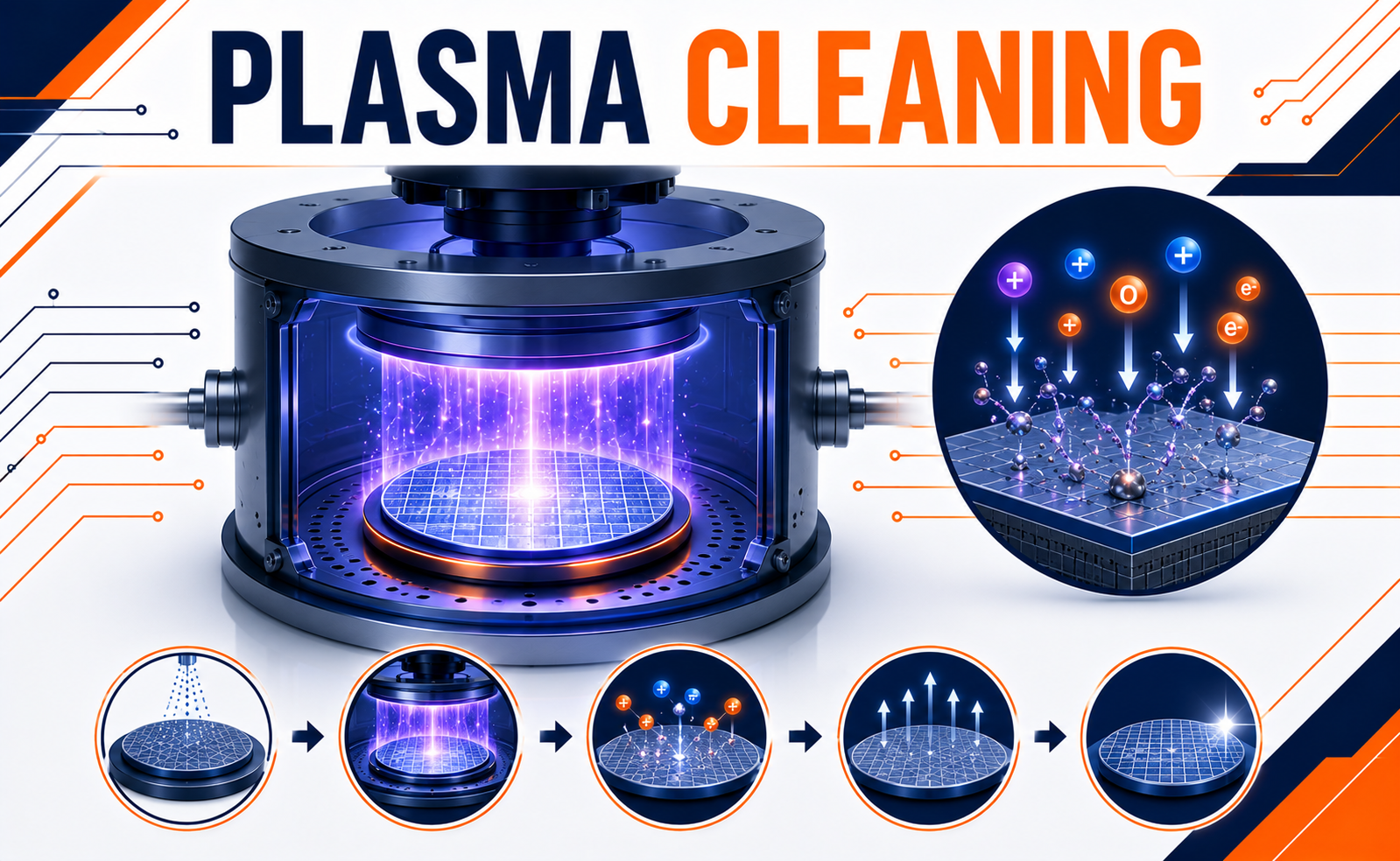
As semiconductor devices continue to shrink to nanometer-scale dimensions, maintaining ultra-clean wafer surfaces has become more critical than ever. Even microscopic organic residues, particles, or contaminants can cause defects, reduce manufacturing yield, and impact the electrical performance of integrated circuits.
Plasma Cleaning is an advanced dry cleaning process widely used throughout semiconductor manufacturing to remove contaminants without damaging sensitive device structures. By utilizing highly reactive plasma species, this technology effectively cleans silicon wafers, photomasks, packaging substrates, and semiconductor components, ensuring optimal adhesion, precise patterning, and reliable device performance.
From advanced logic chips and memory devices to AI processors and 3D packaging technologies, plasma cleaning has become an indispensable process in modern semiconductor fabrication.
What is Plasma Cleaning?
Plasma Cleaning is a dry surface treatment process that uses ionized gases (plasma) to remove organic contaminants, thin oxide layers, moisture, and microscopic particles from semiconductor surfaces.
The plasma contains energetic ions, electrons, radicals, and reactive molecules that chemically react with surface contaminants, converting them into volatile by-products that are safely removed through the vacuum system.
Why Plasma Cleaning is Essential in Semiconductor Manufacturing
Modern semiconductor fabrication requires extremely clean surfaces to ensure reliable device performance and high manufacturing yields.
Plasma cleaning provides several important advantages:
- Removes organic contamination
- Eliminates microscopic particles
- Improves surface wettability
- Enhances thin-film adhesion
- Reduces defect formation
- Improves lithography performance
- Supports nanoscale fabrication
- Minimizes chemical waste compared to wet cleaning
Applications of Plasma Cleaning
Plasma cleaning is used across nearly every stage of semiconductor manufacturing.
Wafer Surface Preparation
Removes contaminants before deposition, oxidation, lithography, and etching processes.
Photolithography
Cleans wafers and photomasks to improve photoresist adhesion and pattern accuracy.
Thin Film Deposition
Prepares surfaces before Chemical Vapor Deposition (CVD), Physical Vapor Deposition (PVD), and Atomic Layer Deposition (ALD).
Advanced Packaging
Enhances bonding quality for flip chip, hybrid bonding, wafer-level packaging (WLP), fan-out packaging, and chiplet integration.
MEMS and Sensor Fabrication
Ensures contamination-free surfaces for microelectromechanical systems and precision sensor manufacturing.
The Future of Plasma Cleaning Technology
As semiconductor manufacturing advances toward sub-2nm process nodes and increasingly complex packaging architectures, plasma cleaning will continue evolving to meet new manufacturing requirements.
Emerging trends include:
- AI-driven plasma process optimization
- Low-damage plasma cleaning technologies
- High-selectivity surface treatment
- Integration with Atomic Layer Processing (ALD and ALE)
- Advanced cleaning for hybrid bonding and chiplet packaging
- Sustainable low-energy plasma systems
- Improved compatibility with High-NA EUV lithography processes
Conclusion
Plasma Cleaning is a cornerstone of modern semiconductor fabrication, providing the ultra-clean surfaces required for advanced lithography, thin-film deposition, etching, packaging, and device integration. Its ability to remove contaminants with exceptional precision while minimizing chemical usage makes it one of the industry’s most valuable surface preparation technologies.
Share your question in comments or talk to our mentor team for batch guidance.
Ask the Admin Team
Drop your basic question in comments: eligibility, prerequisites, tools, fee range, and placement support.
Our team reviews and responds regularly.