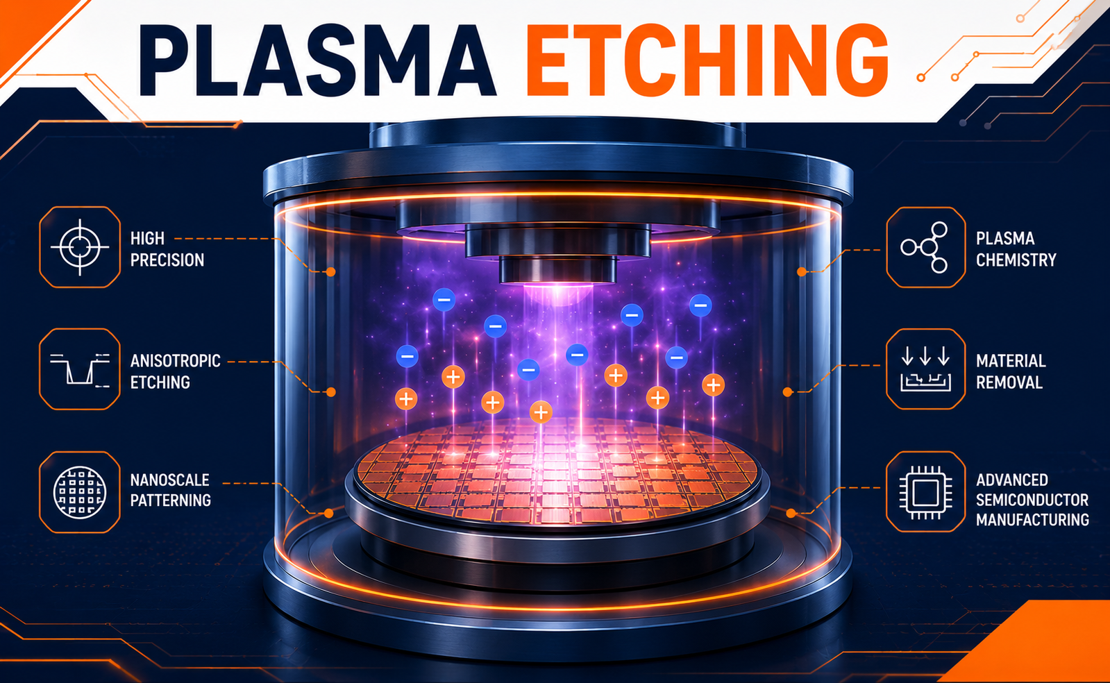
As semiconductor technology advances toward smaller process nodes and increasingly complex device architectures, manufacturing processes require exceptional precision and control. One of the most critical fabrication techniques enabling today’s advanced integrated circuits is Plasma Etching.
Plasma Etching is a highly controlled dry etching process used to selectively remove materials from a semiconductor wafer during chip fabrication. It enables manufacturers to create nanoscale transistor structures, intricate interconnects, and high-aspect-ratio features with outstanding accuracy. From advanced processors and memory chips to AI accelerators and next-generation communication devices, plasma etching plays a vital role in modern semiconductor manufacturing.
What is Plasma Etching?
Plasma Etching is a semiconductor fabrication process that uses ionized gases, known as plasma, to remove selected materials from a wafer surface. The plasma contains energetic ions, electrons, and reactive chemical species that interact with exposed materials, allowing precise etching of microscopic circuit patterns.
Unlike traditional wet chemical etching, plasma etching offers superior control over feature dimensions and enables highly directional material removal, making it ideal for advanced semiconductor devices.
Why Plasma Etching is Essential in Semiconductor Manufacturing
As semiconductor devices continue shrinking below advanced process nodes, manufacturing precision becomes increasingly important.
Plasma etching provides several key advantages:
- Precise nanoscale pattern transfer
- High-aspect-ratio feature fabrication
- Excellent sidewall profile control
- Improved device performance
- Better process uniformity across the wafer
- Reduced contamination compared to wet etching
- Compatibility with advanced lithography techniques
Applications of Plasma Etching
Plasma etching is used throughout the semiconductor fabrication process across a wide range of technologies.
Transistor Fabrication
Forms the intricate structures required for FinFET and Gate-All-Around (GAA) transistor architectures.
Memory Manufacturing
Enables precise etching of high-density DRAM and vertically stacked 3D NAND Flash memory structures.
Interconnect Formation
Creates contact holes, vias, and metal routing patterns that connect billions of transistors within integrated circuits.
MEMS Devices
Produces deep silicon structures used in sensors, microphones, gyroscopes, and accelerometers.
Advanced Packaging
Supports Through-Silicon Via (TSV) formation and high-density interconnect fabrication for 2.5D and 3D packaging technologies.
The Future of Plasma Etching Technology
As semiconductor manufacturing continues evolving toward sub-2nm technologies, plasma etching will remain a core enabling process.
Future developments include:
- Advanced Atomic Layer Etching (ALE) integration
- AI-driven plasma process optimization
- High-selectivity etching chemistries
- Precision fabrication for Gate-All-Around and CFET transistor architectures
- Improved sustainability through lower chemical consumption and energy-efficient processing
- Enhanced compatibility with heterogeneous integration and advanced packaging technologies
Conclusion
Plasma Etching is one of the most important technologies in semiconductor manufacturing, providing the precision required to fabricate today’s advanced integrated circuits. Its ability to create intricate nanoscale structures with exceptional accuracy has made it indispensable for transistor fabrication, memory production, advanced packaging, and next-generation semiconductor devices.
Share your question in comments or talk to our mentor team for batch guidance.
Ask the Admin Team
Drop your basic question in comments: eligibility, prerequisites, tools, fee range, and placement support.
Our team reviews and responds regularly.