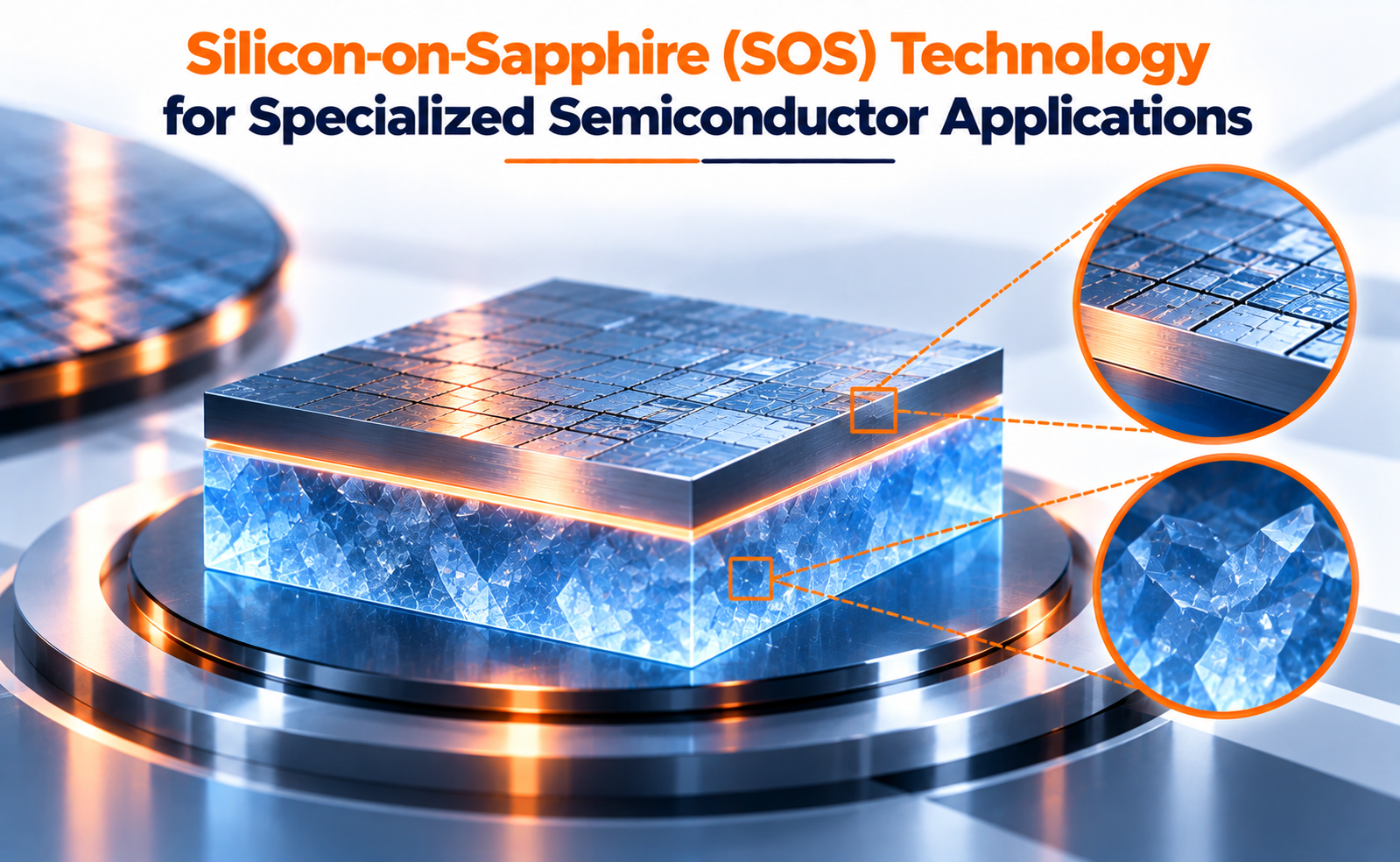
As semiconductor systems expand into demanding applications such as aerospace, defense, radiation-tolerant electronics, and high-frequency communication, conventional bulk-silicon architectures are not always sufficient for every requirement. Silicon-on-Sapphire (SOS) technology provides a specialized semiconductor platform that combines a thin silicon layer with an insulating sapphire substrate.
By providing electrical isolation, low parasitic capacitance, and strong radiation tolerance, SOS technology has become valuable for selected applications where conventional CMOS platforms face unique environmental or electrical constraints.
What Is Silicon-on-Sapphire (SOS) Technology?
Silicon-on-Sapphire is a form of silicon-on-insulator (SOI) technology in which a thin layer of crystalline silicon is formed on top of a sapphire substrate.
A simplified SOS structure consists of:
Silicon Device Layer → Sapphire Interface → Sapphire Substrate
The silicon layer serves as the active semiconductor region where transistors and other devices are fabricated. Sapphire, which is electrically insulating, provides isolation from the underlying substrate.
This structure differs from conventional bulk CMOS, where semiconductor devices are formed directly within a conductive silicon substrate.
The insulating sapphire substrate gives SOS devices several useful characteristics, particularly for applications requiring low parasitic coupling, high isolation, and radiation tolerance.
Key Advantages of SOS Technology
SOS provides several characteristics that make it attractive for specialized semiconductor applications.
Excellent Electrical Isolation
The insulating sapphire substrate significantly reduces unwanted electrical coupling between devices.
Reduced Parasitic Capacitance
The absence of a conductive silicon substrate can reduce certain parasitic capacitances, which can benefit high-speed and low-power circuits.
Radiation Tolerance
SOS structures can provide strong resistance to certain radiation-induced effects, making them useful for selected space and aerospace electronics.
Low Leakage
The electrically isolated substrate can help reduce certain leakage paths compared with conventional bulk-silicon structures.
High-Frequency Capability
Reduced parasitic effects can support high-frequency circuit operation in suitable device architectures.
Applications of Silicon-on-Sapphire Technology
SOS technology is used primarily where its specialized electrical and environmental properties provide meaningful advantages.
Aerospace and Space Electronics
SOS devices can be used in selected systems exposed to radiation and demanding environmental conditions.
Defense Electronics
The technology can support specialized circuits requiring electrical isolation, radiation tolerance, and reliable operation.
RF and High-Frequency Circuits
Low parasitic capacitance and strong isolation can be beneficial for certain radio-frequency and microwave applications.
Radiation-Tolerant CMOS
SOS can be considered for electronics that need increased tolerance to radiation-induced effects.
Low-Power Electronics
Reduced parasitic capacitance can help support low-power circuit designs in suitable applications.
Sensor and Specialized ICs
The electrically isolated substrate can be useful for selected sensing and mixed-signal architectures where substrate coupling needs to be minimized.
The Future of SOS Technology
While mainstream semiconductor manufacturing continues to rely heavily on advanced bulk CMOS and other SOI-based technologies, SOS remains relevant for specialized applications where its unique properties are valuable.
Future SOS development can focus on:
- Improved silicon crystal quality
- Reduced interface defect density
- Better wafer-scale uniformity
- Improved RF performance
- Enhanced radiation tolerance
- More advanced CMOS integration
- Improved manufacturing scalability
- Specialized aerospace and defense applications
SOS can also remain relevant alongside other advanced semiconductor platforms when system designers need a combination of electrical isolation, low parasitics, and environmental robustness.
Conclusion
Silicon-on-Sapphire (SOS) technology is a specialized semiconductor platform that combines a thin silicon device layer with an electrically insulating sapphire substrate. This unique structure provides strong isolation, reduced parasitic effects, and useful radiation-tolerance characteristics.
From aerospace and defense electronics to RF circuits and specialized radiation-tolerant systems, SOS continues to offer capabilities that can be valuable in demanding environments.
Although challenges related to silicon crystal quality, interface defects, thermal stress, manufacturing complexity, and cost remain, advances in epitaxial growth and process control continue to support the development of SOS-based semiconductor technologies.
Share your question in comments or talk to our mentor team for batch guidance.
Ask the Admin Team
Drop your basic question in comments: eligibility, prerequisites, tools, fee range, and placement support.
Our team reviews and responds regularly.