Modern semiconductor devices rely on nearly perfect single-crystal silicon wafers to achieve exceptional electrical performance and manufacturing reliability. As technology nodes continue to shrink and device architectures become increasingly sophisticated, even microscopic crystal imperfections can significantly impact wafer yield, device performance, and long-term reliability.
One of the most important crystal defects encountered during semiconductor manufacturing is the Slip Defect. These defects occur when mechanical or thermal stress causes atomic layers within a silicon crystal to shift along specific crystallographic planes. Understanding, detecting, and preventing slip defects is essential for producing high-quality wafers used in advanced processors, memory devices, AI accelerators, and automotive electronics.
What are Slip Defects?
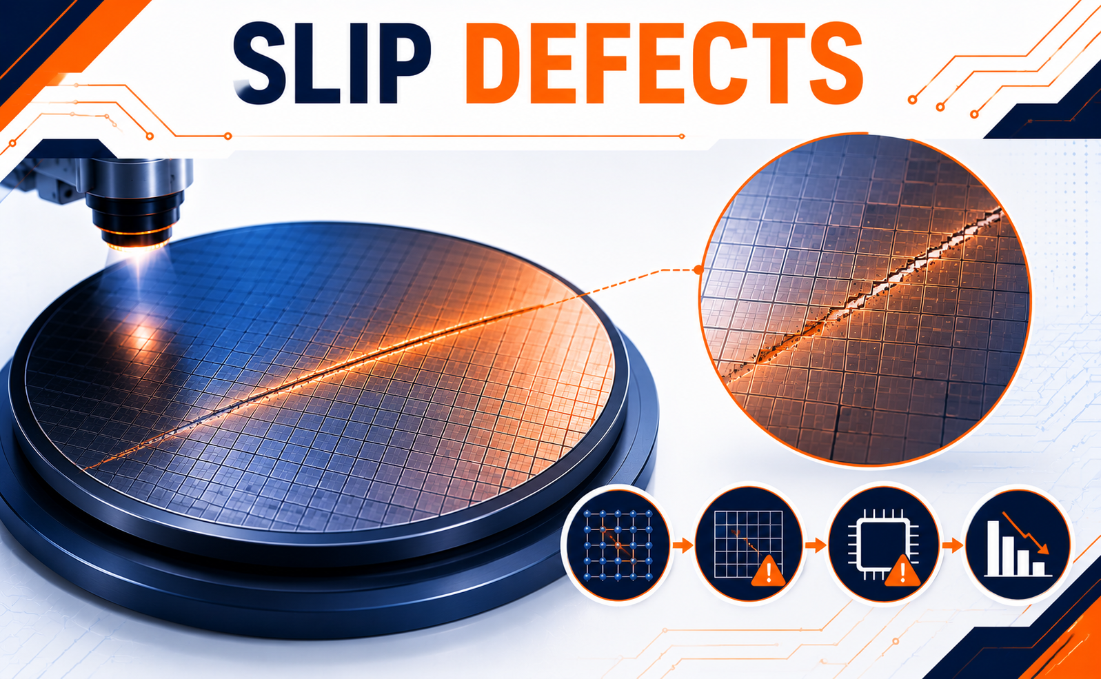
Slip Defects are crystal imperfections that occur when layers of atoms within a single-crystal silicon wafer move relative to one another under excessive mechanical or thermal stress. This movement forms visible dislocation lines known as slip lines, which disrupt the crystal lattice and degrade the wafer’s structural integrity.
Slip defects are typically associated with:
- High-temperature semiconductor processing
- Mechanical handling stress
- Rapid thermal expansion or contraction
- Wafer bending or deformation
- Improper process control
Causes of Slip Defects in Semiconductor Manufacturing
Several factors contribute to the formation of slip defects during wafer fabrication.
Common causes include:
- Rapid heating or cooling during thermal processing
- Non-uniform temperature distribution across the wafer
- Excessive thermal gradients
- Mechanical stress during wafer handling
- Wafer warpage or bending
- Equipment-induced pressure
- High-temperature process conditions
- Crystal imperfections present before fabrication
Detection and Prevention of Slip Defects
Semiconductor manufacturers employ sophisticated inspection and process control techniques to identify and minimize slip defects.
Detection Methods
- Optical wafer inspection
- X-ray topography
- Infrared imaging
- Electron microscopy
- Crystal defect inspection systems
- Automated wafer scanning equipment
Prevention Techniques
- Controlled thermal ramp-up and ramp-down rates
- Uniform wafer heating
- Optimized annealing processes
- Stress-reducing equipment design
- Careful wafer handling automation
- Advanced process monitoring
- Crystal quality optimization during wafer manufacturing
The Future of Slip Defect Control
As semiconductor technology advances toward sub-2nm process nodes and larger wafer sizes, controlling crystal defects becomes increasingly important.
Emerging innovations include:
- AI-driven wafer defect detection
- Real-time thermal stress monitoring
- Predictive process optimization
- Advanced crystal growth technologies
- Improved wafer handling robotics
- High-resolution inspection systems
- Machine learning-based defect analysis
Conclusion
Slip Defects are among the most significant crystal imperfections affecting semiconductor wafer quality. Caused primarily by excessive thermal or mechanical stress, these defects can reduce manufacturing yield, degrade electrical performance, and compromise device reliability.
Share your question in comments or talk to our mentor team for batch guidance.
Ask the Admin Team
Drop your basic question in comments: eligibility, prerequisites, tools, fee range, and placement support.
Our team reviews and responds regularly.