

As semiconductor devices continue to demand higher performance, lower power consumption, and greater functionality, traditional two-dimensional (2D) chip designs are reaching their physical and performance limits. Advanced applications such as Artificial Intelligence (AI), High-Performance Computing (HPC), 5G communications, autonomous vehicles, and data centers require faster data transfer and higher integration density than conventional packaging technologies can provide.
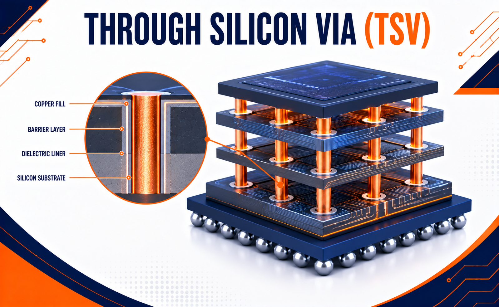
Through-Silicon Via (TSV) is a revolutionary 3D integration technology that enables vertical electrical connections through silicon wafers or dies. By allowing multiple chips to be stacked and interconnected directly, TSV significantly improves bandwidth, reduces signal latency, lowers power consumption, and minimizes package size. Today, TSV is one of the most important technologies driving advanced semiconductor packaging and heterogeneous integration.
What is Through-Silicon Via (TSV)?
A Through-Silicon Via (TSV) is a vertical electrical interconnect that passes completely through a silicon wafer or semiconductor die, creating direct electrical connections between stacked chips.
Unlike traditional wire bonding or flip-chip packaging, TSV technology enables short, high-density vertical interconnections that improve signal integrity and communication speed.
Why TSV Technology is Important
As integrated circuits become increasingly complex, conventional interconnect methods struggle to provide sufficient performance and scalability.
Through-Silicon Via Technology offers several significant advantages:
- High interconnect density
- Extremely short signal paths
- Reduced communication latency
- Higher memory bandwidth
- Lower power consumption
- Smaller package footprint
- Improved electrical performance
- Support for heterogeneous integration
Applications of TSV Technology
Through-Silicon Via technology has become a key enabler for advanced semiconductor packaging.
High-Bandwidth Memory (HBM)
Stacks multiple DRAM dies vertically to deliver extremely high memory bandwidth for AI and HPC applications.
3D Integrated Circuits (3D ICs)
Enables dense vertical integration of logic, memory, and specialized processing components.
Chiplet Architectures
Supports heterogeneous integration by connecting multiple chiplets within advanced packages.
Image Sensors
Used in CMOS image sensors to improve pixel density and reduce package size.
AI, HPC, and Data Centers
Provides high-speed communication between processors, accelerators, and memory devices for demanding computing workloads.
The Future of Through-Silicon Via Technology
As semiconductor packaging continues to evolve, TSV technology will become even more critical for future computing systems.
Emerging developments include:
- Ultra-fine pitch TSV structures
- Integration with hybrid bonding technology
- AI-assisted process optimization
- Chiplet-based heterogeneous integration
- Advanced glass substrate packaging
- Improved thermal management solutions
- Higher-density memory stacking
- Support for next-generation 3D semiconductor architectures
Conclusion
Through-Silicon Via (TSV) technology has transformed semiconductor packaging by enabling high-density vertical interconnections between stacked chips. Its ability to reduce latency, increase bandwidth, improve power efficiency, and support heterogeneous integration makes it one of the most important innovations in modern semiconductor manufacturing.
As the industry advances toward chiplet architectures, AI accelerators, high-bandwidth memory, and 3D integrated circuits, TSV technology will remain a foundational element of next-generation semiconductor systems. By enabling faster communication and greater integration within compact packages, TSV continues to shape the future of advanced electronics.
Share your question in comments or talk to our mentor team for batch guidance.
Ask the Admin Team
Drop your basic question in comments: eligibility, prerequisites, tools, fee range, and placement support.
Our team reviews and responds regularly.