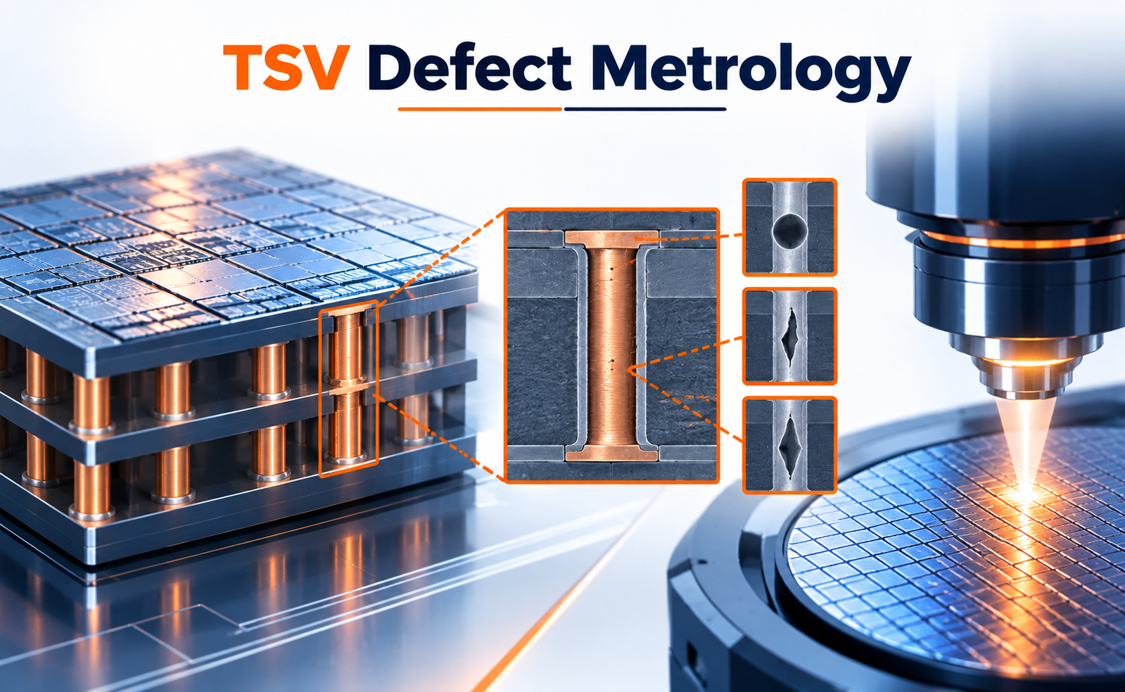
As semiconductor technology moves toward 3D integration, chip stacking, and heterogeneous packaging, Through-Silicon Vias (TSVs) have become an important technology for creating vertical electrical connections between semiconductor dies.
However, TSVs introduce complex manufacturing challenges. Defects such as voids, misalignment, cracks, incomplete fills, and dimensional variations can affect electrical performance and long-term reliability. TSV Defect Metrology provides the measurement and inspection capabilities needed to detect these issues, control process variation, and improve manufacturing yield.
What Is TSV Defect Metrology?
TSV Defect Metrology is the collection of inspection and measurement techniques used to characterize the physical dimensions, structure, and defects of Through-Silicon Vias.
A TSV typically consists of a vertical conductive structure formed through a silicon substrate and insulated from the surrounding silicon. Depending on the manufacturing process, the via may be lined with an insulating layer and filled with copper or another conductive material.
Important TSV parameters include:
- Via diameter and depth
- Via depth-to-width ratio
- Copper fill quality
- Sidewall profile
- Liner thickness
- Via-to-via spacing
- Alignment and placement
- Voids and seams
- Cracks and delamination
- Surface topography
Accurate metrology helps engineers determine whether TSVs meet the required process and reliability specifications.
Why Is TSV Defect Metrology Important?
TSVs are critical electrical pathways in 3D semiconductor structures. Even a small manufacturing defect can create significant problems when multiple dies are stacked together.
Electrical Performance:
Voids, cracks, or incomplete copper fills can increase electrical resistance or interrupt connectivity.
Mechanical Reliability:
Copper and silicon have different coefficients of thermal expansion. Temperature cycling can therefore generate mechanical stress around the TSV.
Process Control:
Metrology data helps engineers identify variations in etching, deposition, insulation, and copper filling processes.
Yield Improvement:
Detecting defects early prevents defective wafers or dies from progressing to expensive downstream packaging stages.
For advanced 3D semiconductor manufacturing, TSV metrology is therefore not simply an inspection step it is an important part of process control and yield management.
Common TSV Defects
Several defect types can occur during TSV fabrication and integration.
Voids and Seams
During copper electroplating, incomplete filling can create internal voids or seams. These defects may compromise electrical and mechanical reliability.
Sidewall Defects
Variations or damage in the etched sidewall can affect liner deposition and subsequent metal filling.
Copper Overburden
Excess copper deposited above the intended surface can create topography problems and increase the requirements for subsequent planarization.
Cracks
Thermal and mechanical stress can produce cracks in the copper, liner, or surrounding silicon.
Misalignment
Incorrect via placement can cause connectivity problems when TSVs must align with other structures or stacked dies.
Dimensional Variation
Changes in via diameter, depth, or profile can affect electrical resistance, capacitance, and mechanical behavior.
Understanding the type, location, and severity of these defects is essential for improving the fabrication process.
The Future of TSV Defect Metrology
As 3D semiconductor integration continues to advance, TSV structures are expected to become more densely packed and increasingly integrated with advanced packaging architectures.
Future TSV metrology will focus on:
- Higher measurement accuracy
- Faster inspection throughput
- Improved internal defect detection
- Automated defect classification
- AI-assisted metrology analysis
- 3D structural characterization
- Real-time process monitoring
- Integration with advanced process-control systems
The ability to detect and understand defects earlier in the manufacturing cycle will become increasingly important as the cost and complexity of advanced semiconductor packaging continue to rise.
Conclusion
TSV Defect Metrology is a critical technology for ensuring the quality and reliability of 3D semiconductor integration. By measuring TSV dimensions, analyzing internal structures, and identifying defects such as voids, cracks, misalignment, and incomplete fills, engineers can improve process control and manufacturing yield.
As semiconductor technology moves toward 3D stacking, chiplets, high-bandwidth memory, and heterogeneous integration, precise TSV characterization will play an increasingly important role in delivering reliable, high-performance semiconductor packages.
Share your question in comments or talk to our mentor team for batch guidance.
Ask the Admin Team
Drop your basic question in comments: eligibility, prerequisites, tools, fee range, and placement support.
Our team reviews and responds regularly.