

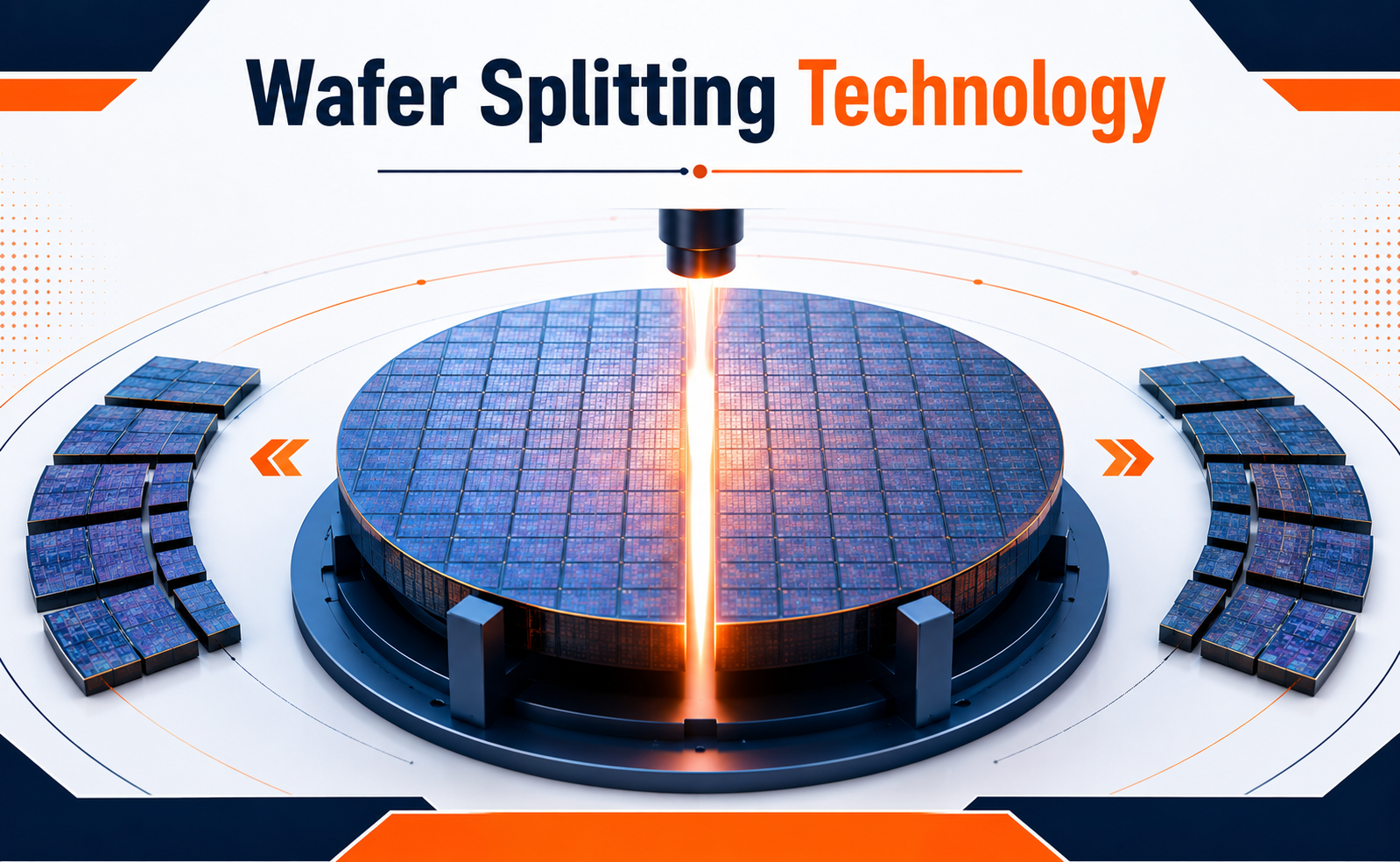
In semiconductor manufacturing, producing a high-quality wafer is only part of the challenge. The wafer must eventually be separated into individual semiconductor dies without damaging the delicate structures created during fabrication. Wafer splitting technology plays an important role in this stage by enabling controlled separation of wafers or die structures with high precision.
As semiconductor devices continue to become smaller and more complex, conventional mechanical separation methods face increasing challenges. Advanced wafer splitting approaches are therefore being developed to improve accuracy, reduce material loss, and protect sensitive device structures.
What Is Wafer Splitting Technology?
Wafer splitting technology refers to techniques used to separate a semiconductor wafer or its individual die regions into controlled sections after fabrication or during specialized processing.
Depending on the wafer material, device structure, and application, splitting can involve different approaches, including:
- Mechanical cleaving and controlled fracture
- Laser-assisted separation
- Plasma or etching-based techniques
- Specialized dicing and wafer separation processes
- Hybrid approaches combining multiple technologies
The primary objective is to achieve clean and predictable separation while minimizing cracks, chipping, contamination, and damage to the active device area.
Why Is Wafer Splitting Important?
Wafer splitting directly influences yield, reliability, manufacturing cost, and device quality.
A poorly controlled separation process can result in:
- Edge chipping and cracks
- Die damage
- Reduced wafer yield
- Material wastage
- Contamination
- Electrical or mechanical reliability issues
Advanced splitting technologies aim to provide cleaner separation with greater repeatability. This becomes particularly important for thin wafers, brittle semiconductor materials, and devices with highly sensitive structures.
For manufacturers, improving wafer separation can contribute to higher usable die counts and more efficient production.
Applications
Advanced IC Manufacturing
Precise separation is important for semiconductor dies containing increasingly dense circuitry.
MEMS Devices
Microelectromechanical systems often contain fragile structures that require carefully controlled separation.
Power Semiconductors
Materials such as silicon carbide and gallium nitride can require specialized approaches because of their material properties.
Optoelectronics
LEDs, photonic devices, and other optical components can benefit from controlled wafer separation.
Advanced Packaging
Wafer-level and heterogeneous packaging processes increasingly depend on precise handling and separation of thin semiconductor structures.
As semiconductor architectures continue to evolve, wafer separation is becoming an increasingly important part of overall manufacturing optimization.
Future of Wafer Splitting Technology
The future of wafer splitting is closely connected to the industry’s transition toward thinner wafers, advanced materials, smaller devices, and higher manufacturing precision.
Emerging approaches are focusing on:
- Lower-damage separation
- Higher throughput
- Improved automation
- Reduced material loss
- Better edge quality
- Integration with advanced inspection systems
- Compatibility with new semiconductor materials
The growing use of wide-bandgap materials and advanced packaging is also creating new requirements for wafer separation. Technologies that can combine precision, productivity, and low defect rates will become increasingly valuable.
Conclusion
Wafer splitting technology is a critical enabling process in modern semiconductor manufacturing. It transforms fabricated wafers into usable semiconductor components while protecting the structures created during earlier manufacturing stages.
As semiconductor devices become thinner, smaller, and more sophisticated, precise wafer separation will play an increasingly important role in improving yield, reliability, efficiency, and manufacturing scalability. Continued innovation in wafer splitting will therefore remain an important part of the semiconductor industry’s push toward next-generation devices.
Share your question in comments or talk to our mentor team for batch guidance.
Ask the Admin Team
Drop your basic question in comments: eligibility, prerequisites, tools, fee range, and placement support.
Our team reviews and responds regularly.