

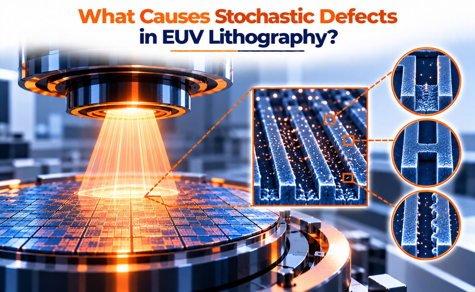
Extreme Ultraviolet (EUV) lithography is a critical technology for manufacturing advanced semiconductor chips with extremely small circuit features. Using light with a wavelength of 13.5 nm, EUV systems can print intricate patterns needed for modern processors, AI accelerators, and high-density memory devices.
However, as these patterns become smaller, manufacturers face a major challenge: stochastic defects. These are random, localized patterning failures caused by microscopic variations in photon absorption, resist chemistry, material composition, and processing conditions.
What Are Stochastic Defects in EUV Lithography?
Stochastic defects are random variations or failures that occur during lithographic pattern formation. They can arise even when the equipment and overall process are operating within their specified limits.
In EUV lithography, these defects are particularly important because the dimensions of printed features approach the scale at which individual photon interactions and molecular-level variations can influence the final pattern.
Common examples include:
- Missing holes: A contact or via opening fails to form correctly.
- Bridging defects: Adjacent resist lines connect where they should remain separated.
- Line breaks: A patterned line develops a gap or discontinuity.
- Line-edge roughness (LER): The edges of a printed feature become irregular.
- Critical dimension (CD) variation: The width or diameter of a feature differs from its intended size.
Photon Shot Noise: Why EUV Exposure Is Inherently Statistical
One of the primary causes of stochastic defects is photon shot noise.
EUV exposure relies on a finite number of photons reaching and being absorbed by the photoresist. Photons arrive and interact with the material in discrete events rather than as a perfectly uniform stream. Consequently, the number of absorbed photons varies across microscopic regions of the resist.
When too few photons are absorbed in a region that must undergo a chemical change, the pattern may not form as intended. In another region, a different number of photon interactions can produce a different chemical response.
These local fluctuations can cause missing holes, irregular line edges, or unwanted connections between neighboring features.
Photon shot noise becomes especially significant when manufacturers attempt to reduce exposure dose, because fewer photons are available to produce the required pattern. Increasing the dose can help reduce some stochastic effects, but it can also reduce production throughput and increase manufacturing cost.
Photoresist Chemistry and Molecular-Level Variations
The photoresist is another major source of stochastic behavior.
A photoresist is a light-sensitive material coated onto the wafer. In chemically amplified resists (CARs), EUV exposure generates chemical species, including acid, that trigger reactions during the post-exposure bake. These reactions change the resist’s solubility, allowing the intended pattern to be developed.
However, the distribution of photoacid generators, quenchers, polymer segments, and other components is not perfectly uniform at the nanoscale.
Several mechanisms contribute to defects:
Nonuniform acid generation: Different regions may generate different amounts of acid because of variations in photon absorption and the local distribution of photoacid generators.
Acid diffusion: During post-exposure baking, acid molecules move through the resist. Excessive or nonuniform diffusion can blur pattern boundaries and increase line-edge roughness.
Chemical reaction variability: Molecular reactions occur probabilistically, so neighboring regions may respond differently even under nominally identical exposure conditions.
Resist composition: Variations in molecular size, component concentration, and material distribution can influence how consistently the resist responds to EUV exposure.
These effects can combine to produce localized pattern failures. Improving resist uniformity and controlling chemical reaction and diffusion behavior are therefore essential for reducing stochastic defects.
Why Do Stochastic Defects Become More Serious at Advanced Nodes?
As semiconductor features shrink, the process becomes less tolerant of local variations.
A small dimensional deviation that has little effect on a larger structure can become critical when a line, contact, or via is extremely small. A tiny bridge may create an electrical short, while a missing contact opening can interrupt an intended connection.
Several factors make stochastic defects particularly challenging at advanced nodes:
Smaller feature dimensions: A single local variation represents a larger fraction of the total feature size.
Reduced process margin: Exposure and development conditions must be controlled within increasingly narrow windows.
Higher pattern density: Closely spaced features require precise control of separation, dimensions, and edge quality.
High-NA EUV requirements: Higher numerical aperture supports finer imaging but introduces additional demands on focus control, resist thickness, and pattern-transfer integration.
Yield sensitivity: Even a low defect probability per feature can become important when a chip contains an enormous number of critical features.
The result is a growing need to reduce defect probability at the individual-feature level, not merely improve average pattern dimensions across the wafer.
Conclusion
Stochastic defects are among the most difficult challenges in EUV lithography because they originate from random events at the photon and molecular scales. Photon shot noise, photoresist chemistry, acid diffusion, development variability, and pattern-transfer effects can all contribute to localized failures.
As semiconductor features continue to shrink, controlling these variations becomes increasingly important for achieving reliable electrical connections and high manufacturing yield.
By improving photoresist materials, optimizing exposure and development conditions, and applying advanced metrology, semiconductor manufacturers can reduce stochastic defectivity and strengthen the manufacturing process for next-generation chips.
Share your question in comments or talk to our mentor team for batch guidance.
Ask the Admin Team
Drop your basic question in comments: eligibility, prerequisites, tools, fee range, and placement support.
Our team reviews and responds regularly.