

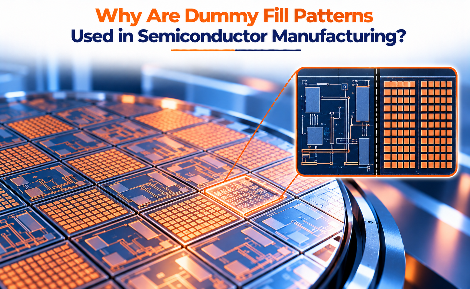
Modern semiconductor manufacturing requires precise control over pattern density, material deposition, and planarization. As integrated circuits become smaller and more complex, even small variations in the layout can affect manufacturing consistency and chip reliability.
Dummy fill patterns are additional geometric shapes inserted into integrated circuit layouts to improve manufacturing uniformity. Although they generally do not perform active electrical functions, they play an important role in processes such as chemical mechanical planarization (CMP), lithography, and advanced interconnect fabrication.
What Are Dummy Fill Patterns?
Dummy fill patterns are non-functional shapes added to regions of a chip layout where the density of functional structures is relatively low. These shapes may appear as small squares, rectangles, or other geometric features distributed across empty layout areas.
They are commonly used in the back-end-of-line (BEOL) process, where metal interconnects are fabricated to connect transistors and other circuit elements.
For example, a layout containing dense metal wiring in one region and very few metal features in another can experience different manufacturing behavior across those regions. Adding dummy metal shapes helps make the pattern density more uniform.
Dummy fill is typically designed to avoid unintended electrical connections, although its exact implementation depends on the layer, technology rules, and design requirements.
Why Dummy Fill Matters in Metal Interconnects
Advanced chips contain multiple metal interconnect layers that connect billions of transistors and other circuit elements.
Variations in metal density can affect deposition, polishing, and subsequent processing steps. Dummy metal fill helps create a more consistent distribution of metal features across these layers.
For example, when a region contains several closely spaced signal wires while another region has large empty spaces, the difference in pattern density can lead to uneven CMP results.
By introducing carefully designed dummy shapes into the sparse region, designers can improve local pattern uniformity.
However, dummy metal must be handled carefully because it can introduce parasitic capacitance, alter local coupling, and affect signal integrity if it is placed too close to sensitive nets.
The Role of Dummy Fill in Lithography and Etching
Dummy fill can also influence patterning behavior during lithography and etching.
Pattern density and neighboring geometries can affect how features print on a wafer. These effects become increasingly important as semiconductor dimensions shrink.
Depending on the process and layer, dummy features can help:
- Make local pattern distributions more uniform.
- Reduce differences between dense and isolated layout regions.
- Support more consistent processing across neighboring structures.
- Improve manufacturability when combined with process-specific design rules.
Dummy fill is not a universal solution for lithography or etch variation. Its impact depends on the process technology, feature geometry, and manufacturing conditions.
Challenges and Design Considerations
Although dummy fill improves manufacturability, indiscriminate insertion can create new problems.
Parasitic capacitance: Dummy metal near functional wires may increase coupling or change signal behavior.
Timing impact: Additional parasitic capacitance can affect delay, especially in timing-sensitive circuits.
Density constraints: Excessive or insufficient fill can violate process-specific minimum and maximum density rules.
Design rule violations: Dummy features must respect spacing, width, enclosure, and other layer-specific restrictions.
Power and signal integrity: Fill placement must account for sensitive analog circuits, high-speed interfaces, clock networks, and other critical structures.
For these reasons, dummy fill is normally generated according to technology-specific rules and validated using physical verification and signoff checks.
Conclusion
Dummy fill patterns are an important part of semiconductor manufacturing because they help improve pattern-density uniformity and support more predictable processing.
By assisting CMP uniformity, reducing certain forms of surface variation, and supporting manufacturing consistency, dummy fill contributes to the reliable fabrication of complex integrated circuits.
However, successful implementation requires a balance between manufacturing requirements and electrical performance. Properly designed and verified dummy fill helps ensure that advanced semiconductor layouts are not only functionally correct but also manufacturable.
Share your question in comments or talk to our mentor team for batch guidance.
Ask the Admin Team
Drop your basic question in comments: eligibility, prerequisites, tools, fee range, and placement support.
Our team reviews and responds regularly.