

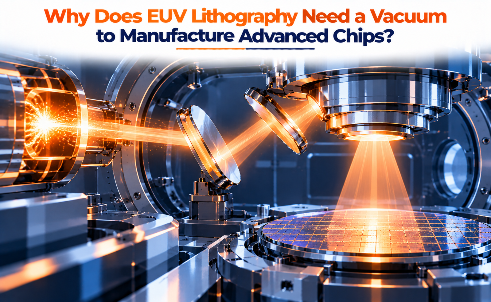
As semiconductor devices become smaller and more powerful, manufacturers need advanced techniques to print increasingly tiny circuit patterns on silicon wafers. Extreme Ultraviolet (EUV) lithography is one of the most important technologies enabling this progress.
EUV lithography uses light with a wavelength of just 13.5 nanometers, allowing manufacturers to pattern some of the most intricate layers in advanced logic and memory chips. However, this extremely short wavelength creates a major engineering challenge: EUV light is readily absorbed by air and many other materials. Consequently, the light must travel through a controlled vacuum environment to reach the wafer effectively.
Why Is EUV Light Easily Absorbed by Air?
EUV light has a much shorter wavelength than the 193 nm light commonly used in deep ultraviolet (DUV) lithography. At 13.5 nm, its interaction with matter is very different from that of visible light.
Air contains molecules that absorb EUV photons. If the light travels through ordinary atmospheric air, much of its energy is lost before reaching the wafer. This would make it difficult to deliver enough light for reliable exposure of the photoresist.
A vacuum greatly reduces the number of gas molecules in the optical path, minimizing absorption and allowing more EUV energy to reach the intended target.
This is the fundamental reason EUV lithography cannot operate like a conventional optical system exposed to normal atmospheric conditions.
Why Does EUV Lithography Use Mirrors Instead of Lenses?
Vacuum alone is not enough. EUV light is also absorbed by ordinary glass, so conventional refractive lenses cannot be used to focus and direct it.
Instead, EUV scanners use highly engineered reflective optics made from multilayer coatings, typically alternating layers of molybdenum and silicon. These layers are carefully designed to reflect light at the required wavelength.
However, each mirror reflects only a portion of the incoming EUV light. As the light passes through multiple optical elements, its intensity decreases. This makes efficient light generation, precise mirror fabrication, and contamination control essential to the overall system.
The vacuum environment helps preserve the EUV beam as it travels from the light source through the illumination optics and patterned mask to the silicon wafer.
What Challenges Does Vacuum Create for Semiconductor Manufacturing?
Although vacuum is essential for EUV lithography, it introduces additional engineering and operational challenges.
Equipment complexity: Vacuum chambers, pumps, seals, and wafer-transfer systems add complexity to the scanner design.
Contamination management: Materials must be carefully selected to minimize outgassing, and optical surfaces must be protected from unwanted deposits.
Thermal and mechanical stability: The optical system and wafer stage require precise control because very small dimensional changes can affect imaging and alignment.
Maintenance and uptime: Maintaining the required environment and protecting sensitive components are important for reliable production.
Light-source debris: The tin plasma used to generate EUV radiation can produce debris that threatens the collector optics. Specialized mitigation and cleaning strategies help manage this issue.
These challenges explain why EUV scanners are among the most sophisticated machines used in modern semiconductor manufacturing.
Why Is Vacuum Technology Important for Future Chip Manufacturing?
As manufacturers advance toward smaller process nodes and more demanding logic and memory designs, EUV lithography continues to play an important role in patterning critical chip layers.
High-NA EUV systems increase the numerical aperture of the optical system to improve imaging resolution. However, these systems still depend on the fundamental requirements of EUV technology: a 13.5 nm light source, specialized reflective optics, precise wafer positioning, and a carefully controlled vacuum environment.
Improvements in vacuum engineering, contamination control, mirror performance, and light-source efficiency will remain important for supporting future semiconductor scaling.
Vacuum technology may operate behind the scenes, but it is a fundamental part of the infrastructure that makes advanced EUV patterning possible.
Conclusion
EUV lithography needs a vacuum because its 13.5 nm light is strongly absorbed by air. The vacuum allows the radiation to travel efficiently through the scanner, while specialized mirrors direct it onto the wafer to form extremely small circuit patterns.
By combining vacuum engineering, precision optics, contamination control, and advanced wafer handling, semiconductor manufacturers can use EUV lithography to produce increasingly sophisticated chips.
Understanding these systems provides valuable insight into the technology behind modern processors, AI accelerators, and high-density memory devices.
Share your question in comments or talk to our mentor team for batch guidance.
Ask the Admin Team
Drop your basic question in comments: eligibility, prerequisites, tools, fee range, and placement support.
Our team reviews and responds regularly.