

Semiconductor manufacturing depends on precise patterning to create the tiny structures that form integrated circuits. During photolithography, a light-sensitive material called photoresist is applied to the wafer and patterned to protect selected areas during subsequent processing.
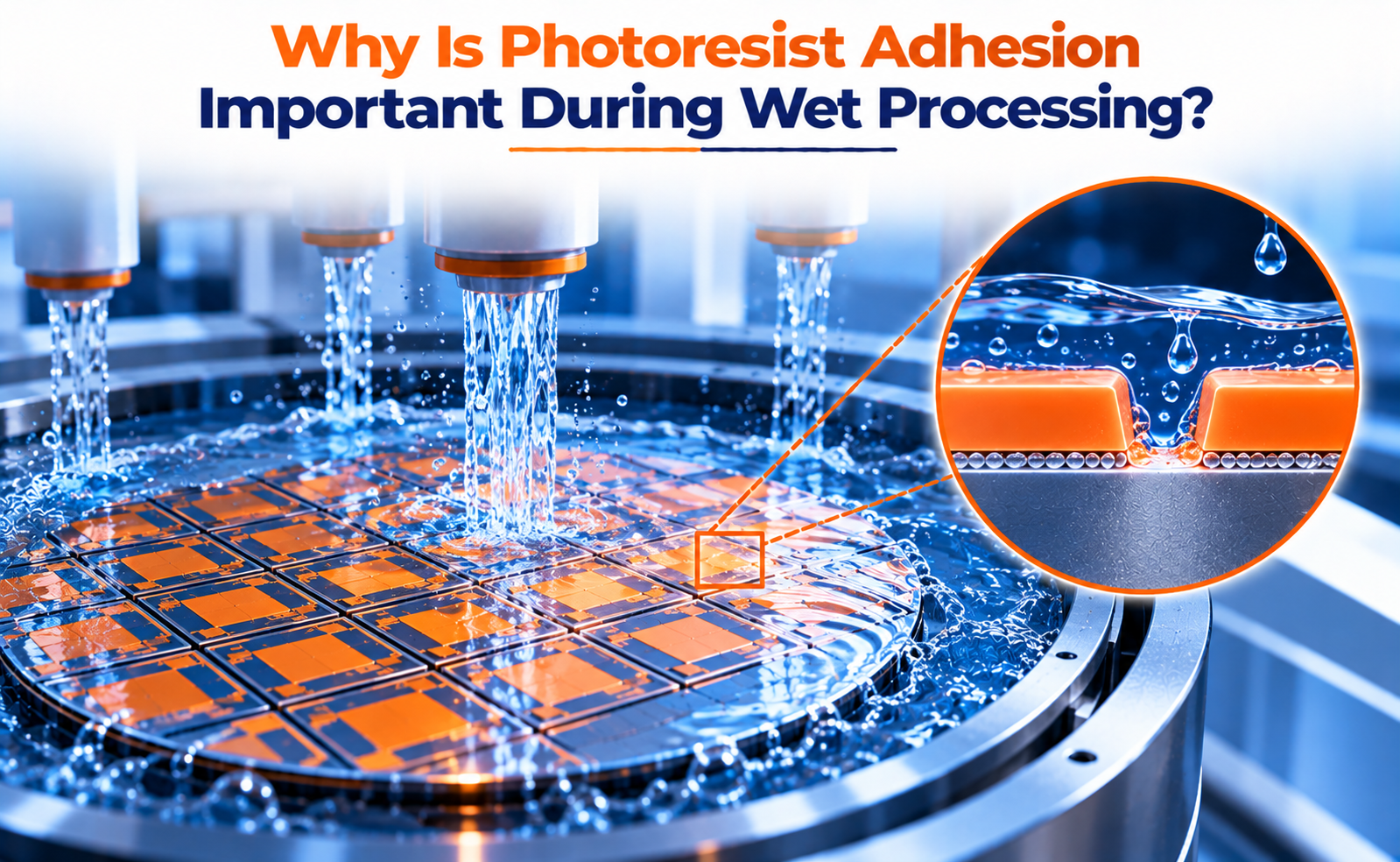
However, the photoresist must remain firmly attached to the wafer throughout wet processing, including chemical development, wet etching, and other liquid-based operations. If the adhesion is weak, chemicals can penetrate beneath the resist, causing pattern defects and compromising the final device.
What Is Photoresist Adhesion?
Photoresist adhesion refers to the ability of a photoresist film to remain attached to the underlying wafer surface during manufacturing.
After photoresist is coated onto a wafer, the desired pattern is created through exposure and development. The remaining resist acts as a protective mask, allowing selected regions to be processed while other regions remain protected.
Strong adhesion is particularly important when the wafer comes into contact with liquids, because moisture and processing chemicals can enter the interface between the resist and the substrate.
The quality of adhesion depends on several factors:
- Wafer surface cleanliness
- Surface moisture and contamination
- Substrate material and surface chemistry
- Photoresist formulation and coating conditions
- Dehydration and baking processes
- Adhesion-promoter treatment
Why Is Adhesion Critical During Wet Processing?
Wet processing exposes the patterned wafer to liquid chemicals that can interact with both the photoresist and the underlying material.
When adhesion is insufficient, liquids may penetrate beneath the resist and weaken its attachment to the surface. This can cause partial lifting, peeling, or complete removal of the patterned film.
Good adhesion helps provide:
- Pattern protection: Keeps the intended regions covered during chemical processing.
- Dimensional accuracy: Reduces unwanted changes to the edges of patterned features.
- Etch control: Helps prevent chemicals from reaching areas that should remain protected.
- Process consistency: Reduces adhesion-related defects across the wafer.
- Improved yield: Helps avoid failures caused by damaged or incorrectly transferred patterns.
These benefits are especially important when manufacturing devices with fine structures and narrow spacing.
What Happens When Photoresist Adhesion Fails?
Poor adhesion can introduce several defects that affect the quality of semiconductor structures.
Photoresist lifting: Small portions of the resist pattern separate from the wafer during development or wet etching.
Undercutting: Etchant penetrates beneath the resist and removes material laterally under the mask, changing the intended feature dimensions.
Pattern deformation: Fine resist lines or small structures may become distorted or disappear.
Chemical penetration: Liquids enter the resist–substrate interface and attack regions that should remain protected.
Yield loss: Defective patterns may cause electrical failures or require wafers to be rejected.
How Do Manufacturers Improve Photoresist Adhesion?
Manufacturers use controlled surface-preparation and coating procedures to strengthen adhesion before the wafer enters subsequent processing steps.
Wafer cleaning
The wafer is cleaned to remove particles, organic residues, and other contaminants that could interfere with contact between the photoresist and substrate.
Dehydration bake
The wafer is heated under controlled conditions to remove adsorbed moisture from its surface. The temperature and duration depend on the substrate and the process requirements.
HMDS priming
Hexamethyldisilazane (HMDS) is a commonly used adhesion promoter for suitable silicon-based and oxide surfaces. It modifies the surface chemistry, making it less hydrophilic and helping reduce moisture-related adhesion problems.
Photoresist coating
The photoresist is applied, commonly through spin coating, to form a uniform film across the wafer.
Soft baking
A controlled bake after coating removes residual solvent and stabilizes the film. The recipe must be appropriate for the specific resist chemistry.
The Role of Adhesion in Wet Etching and Development
Photoresist adhesion is important at different stages of the lithography sequence.
During development: The developer removes the appropriate portions of the exposed or unexposed resist, depending on whether the process uses positive-tone or negative-tone resist. Weak adhesion can cause fine features to lift or disappear.
During wet etching: The photoresist serves as a mask over protected areas. If the resist lifts, the etchant may reach material that should not be removed.
During rinsing and drying: Liquid movement and the drying process can reveal weaknesses in the resist film or contribute to defects when the process is poorly controlled.
During subsequent processing: A damaged mask may compromise later operations, leading to dimensional errors or defective device structures.
Reliable adhesion therefore supports accurate pattern transfer from the lithography step to the underlying material.
How Can Adhesion-Related Defects Be Prevented?
Preventing adhesion problems requires monitoring both wafer preparation and the photoresist process.
Important practices include:
- Maintain effective wafer-cleaning procedures.
- Minimize the time a prepared wafer remains exposed to ambient contamination.
- Verify dehydration-bake conditions.
- Optimize HMDS priming for the substrate and resist system.
- Follow the photoresist manufacturer’s recommended coating and baking conditions.
- Inspect developed patterns for lifting, peeling, missing features, and edge defects.
- Monitor process conditions, including humidity, where relevant.
If adhesion defects appear repeatedly, engineers should investigate the wafer surface, priming process, resist chemistry, and bake conditions rather than assuming that a single process adjustment will solve the problem.
Conclusion
Photoresist adhesion is a fundamental requirement for reliable semiconductor wet processing. Strong adhesion helps the patterned resist remain in place while developers and etchants perform their intended functions.
By controlling surface cleanliness, moisture, adhesion-promoter treatment, coating, and baking, semiconductor manufacturers can reduce pattern lifting, undercutting, and other resist-related defects.
Share your question in comments or talk to our mentor team for batch guidance.
Ask the Admin Team
Drop your basic question in comments: eligibility, prerequisites, tools, fee range, and placement support.
Our team reviews and responds regularly.