

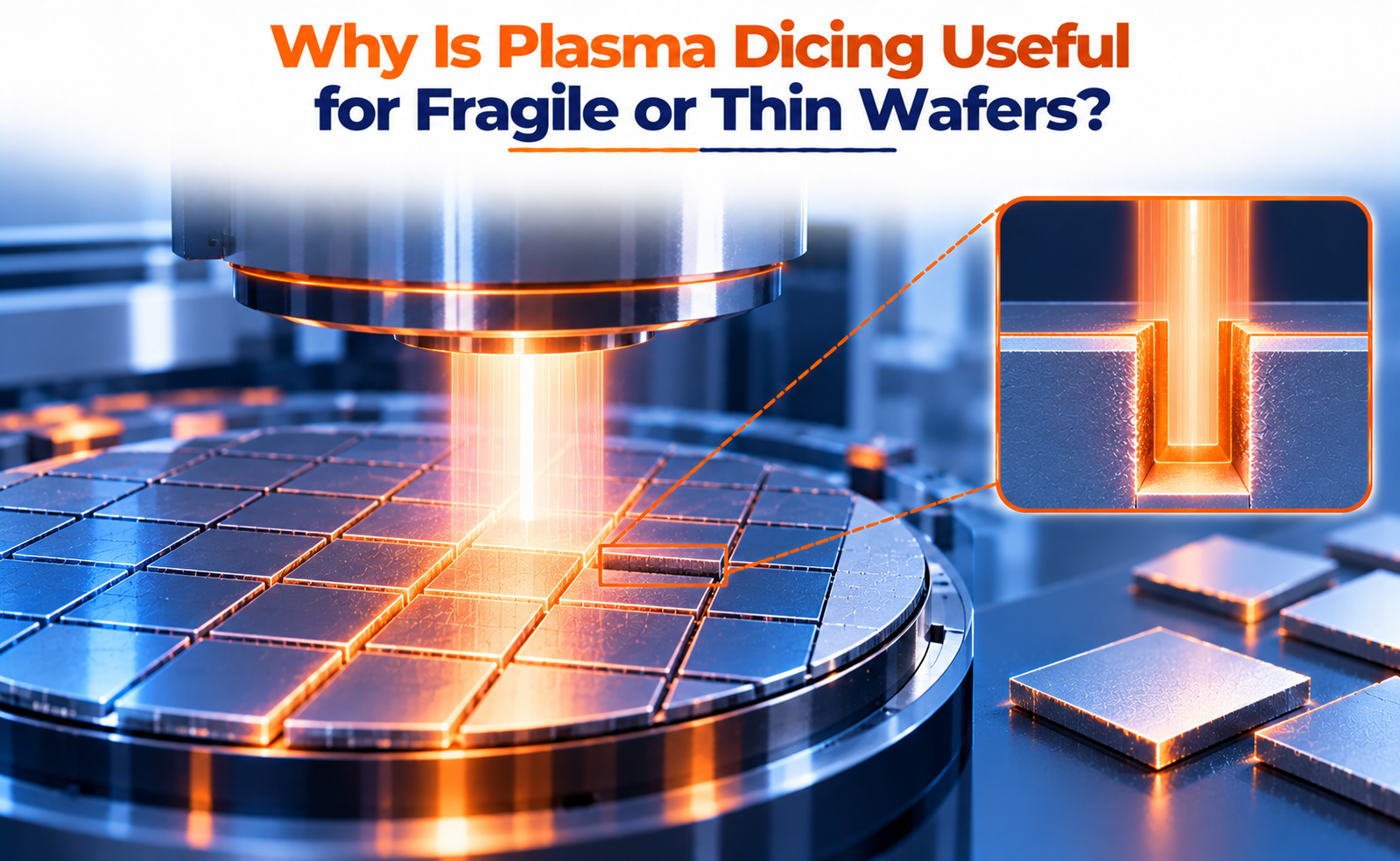
Plasma dicing is an advanced semiconductor singulation technique that separates individual chips from a wafer using plasma-based etching rather than relying entirely on a mechanical saw. It is particularly useful for fragile or thin wafers because it can reduce mechanical stress, minimize edge damage, and support the formation of narrow separation streets. These advantages make plasma dicing attractive for applications requiring delicate die handling, precise geometry, and reliable chip separation.
What Is Plasma Dicing in Semiconductor Manufacturing?
Plasma dicing is a wafer singulation technique that uses chemically reactive plasma to etch narrow streets between individual semiconductor dies. Unlike conventional blade dicing, which physically cuts the wafer with a rotating blade, plasma dicing removes material through controlled chemical reactions.
Before dicing, a suitable mask is patterned on the wafer to expose the intended separation streets while protecting the device regions. The wafer is then placed in a plasma etching system, where reactive species remove silicon along the exposed paths.
This process can separate multiple die streets in parallel rather than cutting each street sequentially with a blade.
Plasma dicing is particularly attractive for thin silicon wafers, fragile low-k dielectric structures, MEMS devices, and advanced packaging applications where mechanical damage and contamination must be minimized.
Why Are Thin and Fragile Wafers Difficult to Dice?
As semiconductor wafers become thinner, they become more susceptible to mechanical stress, bending, cracking, and breakage during handling and singulation.
Traditional blade dicing introduces physical contact and cutting forces. These forces can create localized stress near the cut edge, potentially producing chipping, microcracks, and damaged sidewalls.
Several factors make thin wafers especially challenging to process:
- Reduced mechanical strength: A thin wafer or die is less tolerant of bending and handling forces.
- Edge chipping: Mechanical cutting can remove small fragments from the wafer edge.
- Microcrack formation: Small cracks can develop near the cut and propagate during subsequent handling or packaging.
- Residual stress: Wafer thinning and previous fabrication processes can leave stresses that increase the risk of fracture.
- Fragile device structures: Low-k dielectrics, MEMS structures, and delicate interconnects may be damaged by mechanical forces or debris.
These risks become more important in advanced packaging, where ultra-thin dies must survive die bonding, stacking, and subsequent assembly operations.
How Does Plasma Dicing Reduce Mechanical Damage?
The main advantage of plasma dicing is its non-contact material-removal mechanism.
Instead of forcing a blade through the wafer, the process uses reactive species generated in a plasma to etch exposed material along predefined streets. Because there is no rotating cutting blade pressing against the wafer, the process avoids the mechanical cutting forces associated with conventional sawing.
This provides several benefits.
Reduced chipping and microcracking: Removing material through chemical etching can reduce the edge damage associated with mechanical cutting.
Improved die strength: Lower mechanical damage at die edges can improve the ability of separated dies to withstand subsequent handling and assembly.
Reduced cutting debris: Plasma etching primarily produces reaction by-products that can be removed through the process exhaust system, reducing the particulate debris associated with mechanical cutting.
Narrower dicing streets: Plasma-based etching can support narrower separation paths, reducing the wafer area consumed by dicing.
Support for delicate structures: The absence of blade contact makes plasma dicing attractive for fragile MEMS structures and selected advanced packaging applications.
Why Is Plasma Dicing Valuable for Advanced Packaging?
Advanced semiconductor packaging increasingly relies on thin dies, dense interconnects, and compact multi-die assemblies. In these applications, die-edge quality can affect both manufacturing yield and long-term package reliability.
Plasma dicing offers several advantages for these demanding requirements.
Higher die strength: Reduced mechanical damage at the cut edge can help dies withstand subsequent handling and assembly.
Improved usable wafer area: Narrower dicing streets may allow more dies to fit on a wafer, depending on the layout and process constraints.
Cleaner processing: Reduced mechanical debris can be valuable when clean surfaces are important for die bonding and hybrid bonding.
Flexible die shapes: Plasma etching can accommodate selected non-rectangular die geometries when the mask and process are designed accordingly.
Parallel processing: Multiple dicing streets can be etched during the same process, making the approach attractive for wafers containing many small dies.
These capabilities are relevant to applications such as high-bandwidth memory, stacked dies, image sensors, MEMS devices, and other advanced semiconductor packages.
However, the benefits vary with die size, wafer material, etch depth, equipment configuration, and process throughput. Narrower streets and higher die strength do not automatically guarantee higher yield in every application.
What Are the Challenges and Limitations of Plasma Dicing?
Despite its advantages, plasma dicing introduces process and equipment challenges that must be considered before implementation.
Etch selectivity: The plasma chemistry must remove the target material without damaging protected device regions, exposed films, or underlying structures.
Mask integrity: The mask must remain effective throughout the etching process, especially when the wafer is thick or the streets require deep etching.
Sidewall quality: Inadequately optimized etch and passivation conditions can produce roughness, notching, or undercutting that affects die strength.
Material compatibility: Multilayer wafer structures containing different materials may require specialized chemistries and additional process development.
Process cost: Plasma dicing requires dedicated equipment, mask preparation, and recipe optimization. Its economic advantage depends on throughput, die size, wafer thickness, and yield improvement.
Handling and carrier requirements: Very thin wafers often require tape, temporary bonding, or other support methods to remain stable during processing and separation.
For these reasons, plasma dicing is not a universal replacement for blade or laser dicing. Manufacturers select the singulation method according to the wafer material, device structure, die geometry, production volume, and reliability requirements.
Conclusion
Plasma dicing is particularly useful for fragile or thin wafers because it separates semiconductor dies through controlled plasma etching rather than mechanical blade contact. This can reduce edge chipping, microcracks, cutting debris, and mechanical stress while supporting narrow dicing streets and improved die strength.
Its value is especially clear in applications involving ultra-thin silicon, delicate MEMS structures, and advanced multi-die packaging. However, successful implementation still requires careful control of etch chemistry, mask integrity, sidewall quality, and wafer handling.
As semiconductor packages continue to become thinner and more densely integrated, plasma dicing provides an important option for improving die quality and supporting reliable manufacturing.
Share your question in comments or talk to our mentor team for batch guidance.
Ask the Admin Team
Drop your basic question in comments: eligibility, prerequisites, tools, fee range, and placement support.
Our team reviews and responds regularly.