

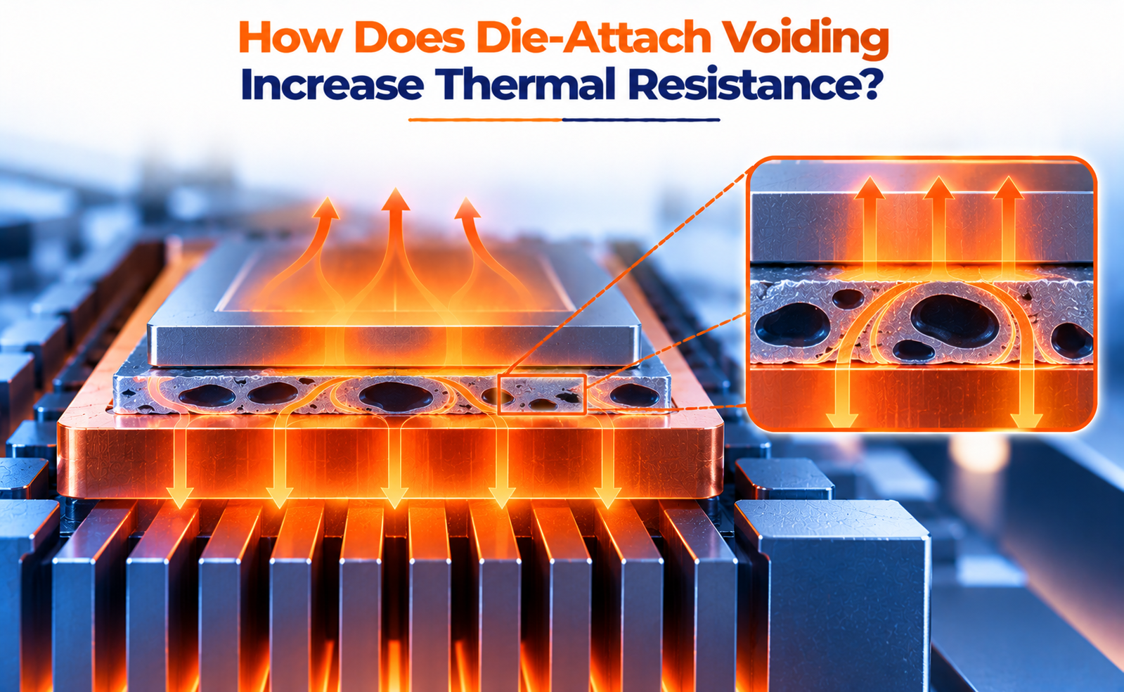
As semiconductor devices become more powerful and compact, removing heat efficiently becomes a critical part of package design. Power amplifiers, processors, automotive electronics, and high-performance semiconductor devices can generate significant heat during operation. If this heat is not transferred efficiently from the silicon die to the package or heat sink, the device temperature can rise and affect performance, reliability, and operating lifetime.
One important factor that affects heat dissipation is die-attach voiding. Voids are unwanted empty regions or gas-filled pockets within the material that bonds a semiconductor die to its supporting substrate or package. Although these defects may appear small, they can disrupt heat flow and increase the thermal resistance of the package.
What Is Die Attach in Semiconductor Packaging?
Die attach is the process of bonding a semiconductor die to a supporting structure, such as a leadframe, package substrate, or heat spreader.
The die-attach material provides mechanical support and, depending on the package design, may also provide an electrical connection and a thermal path for heat dissipation.
Common die-attach materials include:
- Epoxy adhesives: Used for bonding dies in a wide range of semiconductor packages.
- Silver-filled adhesives: Provide improved thermal conductivity compared with many conventional polymer adhesives.
- Solder alloys: Used where a conductive, thermally efficient bond is required.
- Sintered silver: Used in selected high-power applications because of its potential for high thermal conductivity and reliable heat transfer.
During die attach, the bonding material should form a sufficiently uniform interface between the die and the underlying surface. Poor material coverage, trapped gas, contamination, or an unsuitable bonding process can lead to void formation.
These voids interrupt the intended heat-transfer path between the semiconductor die and the package.
What Is Die-Attach Voiding?
Die-attach voiding occurs when portions of the bonding interface contain empty spaces instead of the intended die-attach material.
Voids can form because of several factors:
- Trapped air or gas during material dispensing or bonding.
- Moisture or volatile compounds released during heating.
- Inadequate wetting of the die or substrate surface.
- Incorrect bonding pressure, temperature, or curing conditions.
- Contamination or surface irregularities.
- Process variations during soldering or sintering.
Voids can vary in size, shape, location, and distribution. Some are isolated, while others form clusters or extend across larger portions of the interface.
Their impact depends not only on the total void percentage but also on where the voids are located. A void beneath a high-heat-flux region can be more harmful than a similarly sized void near the edge of a die.
How Do Voids Create Localized Hotspots?
Heat generated inside a semiconductor die must travel through the die-attach layer before reaching the package structure or heat sink.
When the interface contains voids, heat flow becomes uneven. Regions with good material contact continue to conduct heat, while voided regions provide a less effective thermal path.
This can lead to localized temperature increases.
For example, consider a power semiconductor die with a high-heat-flux region near its center. If a large void forms directly underneath that region, the heat has fewer effective paths into the package. The local temperature may rise even when the overall void percentage appears acceptable.
Localized hotspots can contribute to:
- Higher junction temperatures.
- Uneven temperature distribution across the die.
- Increased thermomechanical stress.
- Accelerated degradation of materials and interfaces.
- Reduced operating margins and reliability.
The severity depends on the device’s power density, package construction, material properties, cooling conditions, and the position and shape of the voids.
rea fraction.
Scanning acoustic microscopy
Acoustic inspection can help identify delamination and interface defects. Its effectiveness depends on the package structure, the location of the defect, and the acoustic properties of the materials.
Thermal characterization
Thermal measurements and simulations help evaluate how interface defects affect heat transfer. Methods such as transient thermal testing can provide insight into the thermal behavior of the package.
Process optimization
Void formation can be reduced by improving surface preparation, controlling material dispensing, optimizing bonding pressure and temperature, managing moisture, and refining curing, reflow, or sintering conditions.
Thermal simulation
Finite-element analysis and other thermal models can estimate temperature distributions and identify sensitive regions. Including realistic void locations and geometries can help engineers assess their impact more accurately.
Acceptance limits should be defined according to the package design, material system, power requirements, and applicable reliability standards. A single void-percentage threshold is not appropriate for every semiconductor package.
Conclusion
Die-attach voiding increases thermal resistance by replacing highly conductive bonding material with regions that transfer heat less effectively. These voids reduce effective heat-transfer area, distort heat-flow paths, and can create localized hotspots beneath the semiconductor die.
The resulting temperature rise may affect device performance, accelerate material degradation, and reduce package reliability, particularly in high-power applications.
By controlling the die-attach process, inspecting bonded interfaces, and evaluating thermal performance, semiconductor manufacturers can reduce void-related risks and improve heat dissipation.
Share your question in comments or talk to our mentor team for batch guidance.
Ask the Admin Team
Drop your basic question in comments: eligibility, prerequisites, tools, fee range, and placement support.
Our team reviews and responds regularly.