

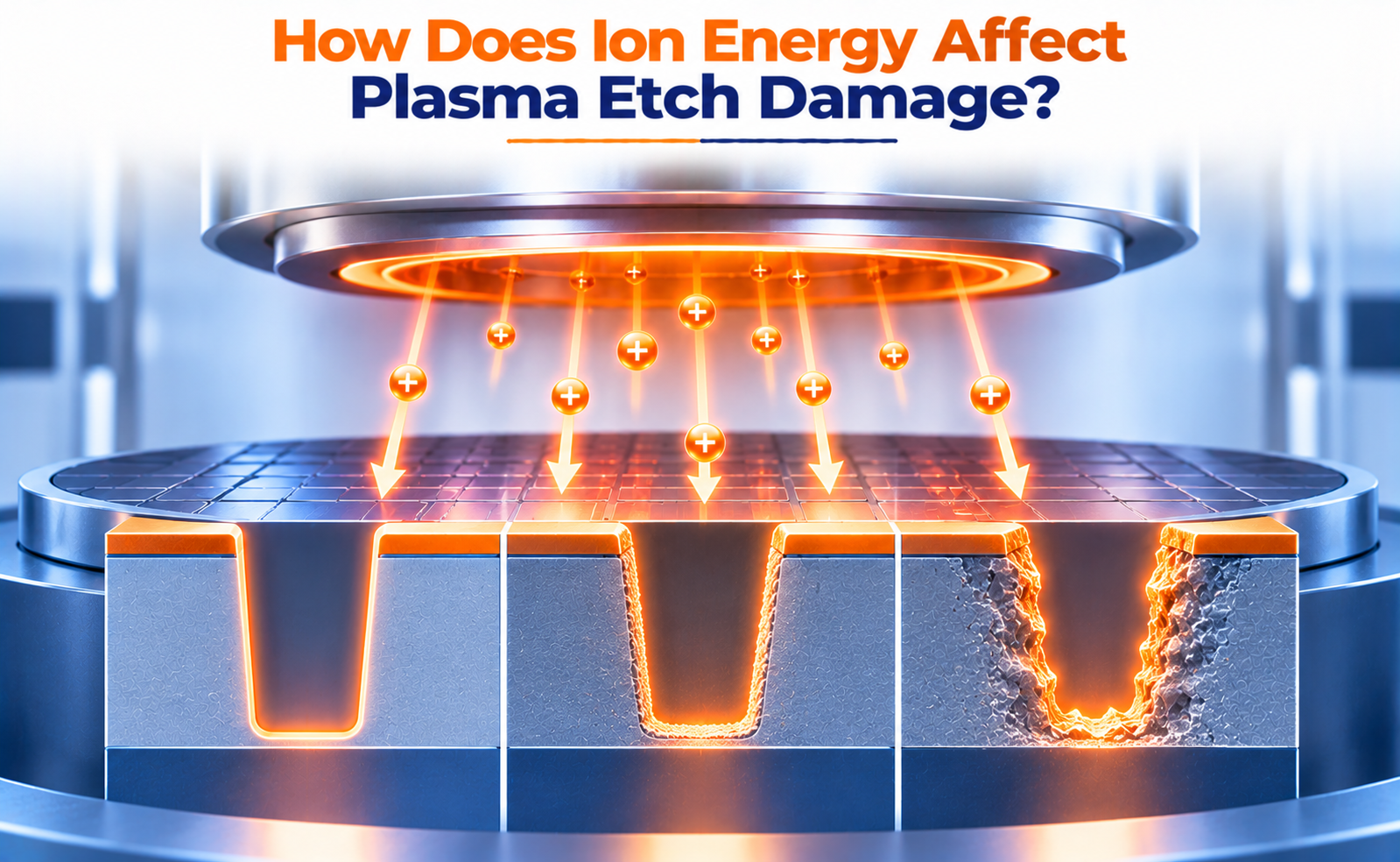
Plasma etching is a critical process in semiconductor manufacturing, used to create precise patterns, trenches, contact holes, and microscopic structures on silicon wafers. During this process, ions generated inside the plasma are accelerated toward the wafer surface, helping remove material and achieve directional etching.
However, the energy carried by these ions must be carefully controlled. While sufficient ion energy improves material removal and etch anisotropy, excessive energy can damage the semiconductor surface, create lattice defects, and affect the electrical characteristics of devices.
Understanding how ion energy influences plasma etch damage is essential for developing reliable and high-performance semiconductor manufacturing processes.
What Is Ion Energy in Plasma Etching?
Ion energy refers to the kinetic energy carried by charged particles as they travel toward and strike the wafer surface during plasma processing.
Inside a plasma chamber, process gases are ionized to generate positive ions, electrons, and reactive neutral species. An electrical potential develops near the wafer surface, known as the plasma sheath.
Positive ions accelerate across this sheath and bombard the wafer.
The energy of these ions is influenced by several process parameters:
- RF bias power: Controls the electrical bias applied to the wafer and strongly influences ion bombardment energy.
- Chamber pressure: Affects collisions within the sheath and can influence the ion energy and angular distributions.
- Plasma density: Influences ion flux and the overall number of ions reaching the wafer.
- Gas chemistry: Determines the types of ions and reactive species present in the plasma.
- Substrate conditions: Wafer materials and electrical properties influence how plasma exposure affects the surface.
Ion energy is commonly expressed in electronvolts (eV). Its distribution, rather than just a single average value, is important when evaluating the behavior of ions during etching.
Why Is Ion Energy Important for Material Removal?
Ion bombardment helps remove material from the wafer through physical sputtering and ion-enhanced chemical reactions.
In plasma etching, these mechanisms work together to achieve the required etch rate and profile.
Physical sputtering: Energetic ions transfer momentum to surface atoms. When sufficient energy is transferred, atoms can be ejected from the material.
Ion-enhanced chemical etching: Ion bombardment activates surface reactions, breaks chemical bonds, and helps remove reaction products.
Anisotropic etching: Directional ion bombardment assists vertical material removal while suitable passivation chemistry protects the sidewalls.
When ion energy is appropriately controlled, engineers can achieve accurate feature dimensions, vertical sidewalls, and effective material removal.
However, increasing ion energy beyond the required process window can cause excessive physical bombardment and unwanted surface damage.
The objective is therefore to provide enough energy for controlled etching without unnecessarily disturbing the underlying semiconductor material.
What Happens When Ion Energy Is Too Low or Too High?
Ion energy must be optimized according to the material and the intended etching mechanism.
Both insufficient and excessive ion energy can create manufacturing challenges.
When ion energy is too low
- Incomplete removal of surface reaction products.
- Reduced etch rate in ion-assisted processes.
- Poor etch anisotropy.
- Residual material at the bottom of etched features.
- Difficulty maintaining the required feature profile.
When ion energy is too high
- Increased physical sputtering.
- Greater risk of lattice displacement and surface damage.
- Increased surface roughness.
- Reduced selectivity between the target and underlying materials.
- Potential degradation of electrical properties.
How Does Ion Energy Affect Electrical Device Performance?
Plasma etch damage is not limited to visible surface defects. It can also change the electrical behavior of semiconductor devices.
When ions create defects near the surface, they may introduce electrically active states that influence carrier movement and device operation.
Some important consequences include:
Increased leakage current: Surface defects and damaged interfaces can create additional leakage paths.
Threshold voltage variation: Plasma-induced defects and charge trapping can influence the electrical characteristics of MOS transistors.
Carrier mobility degradation: Defects and surface roughness can increase carrier scattering and reduce effective mobility.
Gate dielectric reliability issues: Plasma-induced charging and energetic particle exposure can affect thin insulating layers.
Reduced device lifetime: Defect formation and interface degradation can contribute to long-term reliability problems.
What Techniques Help Reduce Ion-Induced Etch Damage?
Semiconductor manufacturers use several approaches to control ion energy while maintaining the required etch performance.
Optimize RF bias power
Adjusting wafer bias helps control the energy delivered by incoming ions. Reducing excessive bias can lower physical bombardment and minimize lattice damage.
Use high-density plasma sources
Inductively coupled plasma (ICP) systems can provide relatively high plasma density while allowing ion energy to be controlled through a separate substrate bias.
This helps engineers maintain an adequate ion flux without necessarily increasing ion energy.
Apply pulsed plasma processing
Pulsed plasma techniques periodically switch plasma conditions to influence ion bombardment, charging behavior, and surface reactions.
Depending on the process, this can help reduce plasma-induced damage while maintaining etch performance.
Use atomic layer etching
ALE separates surface modification and material removal into controlled steps. In plasma-enhanced ALE, low-energy ion bombardment removes the modified surface layer while minimizing damage to the underlying material.
Optimize gas chemistry
Selecting appropriate etch gases helps balance chemical reactions and physical bombardment. Increasing the chemical contribution can sometimes reduce the need for excessive ion energy.
Apply suitable post-etch treatments
Depending on the material system, thermal annealing, surface cleaning, or other recovery treatments may help remove residues or reduce certain forms of plasma-induced damage.
Conclusion
Ion energy plays a fundamental role in determining both the effectiveness and the potential damage associated with plasma etching.
Appropriate ion energy supports directional material removal, improves etch profiles, and enables precise pattern transfer. Excessive energy, however, can cause lattice defects, surface amorphization, roughness, implantation, and electrical degradation.
By optimizing RF bias, plasma density, gas chemistry, and etching techniques, semiconductor manufacturers can achieve a balance between etch performance and surface protection.
Share your question in comments or talk to our mentor team for batch guidance.
Ask the Admin Team
Drop your basic question in comments: eligibility, prerequisites, tools, fee range, and placement support.
Our team reviews and responds regularly.