

In semiconductor manufacturing, plasma etching is widely used to create narrow trenches, contact holes, and other microscopic structures. These features must have accurate dimensions and well-controlled sidewall profiles to ensure reliable device operation.
However, during anisotropic plasma etching, an unwanted defect called microtrenching can develop near the bottom corners of an etched feature. Instead of producing a relatively flat trench bottom, the process creates small, localized grooves near the sidewalls.
Microtrenching can affect profile uniformity, damage underlying layers, and create challenges during subsequent fabrication steps. Understanding its formation mechanism is important for achieving precise etch profiles in advanced semiconductor manufacturing.
What Is Microtrenching in Semiconductor Etching?
Microtrenching is a plasma-etching defect characterized by localized excessive material removal near the bottom corners of a trench or etched feature.
Ideally, an anisotropic etching process should produce nearly vertical sidewalls and a reasonably uniform bottom surface. However, when microtrenching occurs, the bottom corners are etched more deeply than the central region.
This produces a characteristic groove-like or V-shaped profile near the base of the structure.
Microtrenching can occur during reactive ion etching (RIE) and inductively coupled plasma (ICP) etching, depending on the material, plasma chemistry, feature geometry, and operating conditions.
It is particularly important in processes involving:
- Deep silicon trench etching.
- High-aspect-ratio contact formation.
- Dielectric trench etching.
- Silicon carbide (SiC) device fabrication.
- Advanced pattern-transfer processes.
The defect is associated with an increased local etch rate near the bottom corners rather than uniform material removal across the entire trench floor.
Why Does Microtrenching Occur Near the Bottom Corners?
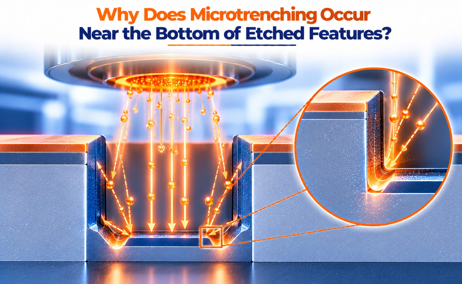
One of the primary mechanisms responsible for microtrenching is the reflection and scattering of energetic ions from the trench sidewalls.
During plasma etching, positively charged ions are accelerated toward the wafer surface by the electric field in the plasma sheath. Their trajectories are generally directed toward the wafer, supporting anisotropic etching.
However, ions do not always travel in perfectly vertical paths.
Some ions have small angular deviations. When they strike a trench sidewall, they can undergo reflection or scattering.
Under suitable conditions, these energetic particles are redirected toward the lower corners of the trench.
This produces a locally increased ion flux and enhances material removal near the bottom edges.
The sequence can be understood as follows:
- Ions travel toward the wafer during plasma etching.
- Some ions strike the trench sidewalls instead of reaching the bottom directly.
- These ions undergo reflection or scattering.
- A portion of the redirected ions reaches the bottom-corner regions.
- Localized ion bombardment increases the etch rate near those corners.
- Small grooves develop along the bottom edges.
What Process Parameters Influence Microtrenching?
Microtrenching is influenced by several plasma-processing parameters. Controlling these parameters helps engineers reduce localized over-etching and improve profile uniformity.
RF bias power
RF bias power influences the energy with which ions bombard the wafer.
Higher ion energy can increase physical sputtering and sidewall reflection effects. In some processes, increasing bias power has been associated with deeper microtrenches.
Careful bias optimization is therefore important for controlling excessive ion bombardment.
Chamber pressure
Pressure affects the frequency of collisions between particles in the plasma.
At different pressures, the angular distribution and energy of ions reaching the wafer can change. These variations influence how particles interact with trench sidewalls.
Plasma source power
Source power influences plasma density and ion flux. Changes in ion flux can affect the rate and uniformity of material removal.
Gas chemistry
Etch gases determine the balance between chemical reactions, physical bombardment, and sidewall passivation.
For example, fluorine-based and chlorine-based plasma chemistries can produce different etching behaviors depending on the material being processed.
Substrate temperature
Temperature influences surface reaction rates, by-product removal, and the formation or stability of passivation layers.
How Can Microtrenching Be Reduced?
Semiconductor manufacturers use several process-control techniques to minimize microtrenching while maintaining the required etch rate and profile.
Optimize RF bias power: Reducing excessive ion energy can help minimize energetic sidewall bombardment and reflection.
Control ion angular distribution: Plasma and sheath conditions can be optimized to improve directional ion transport toward the wafer surface.
Improve sidewall passivation: Suitable passivation chemistry can protect trench sidewalls and modify particle interactions near the bottom corners.
Optimize chamber pressure: Adjusting pressure can influence ion scattering and angular distribution, helping improve profile uniformity.
Use pulsed plasma techniques: Modulating plasma operation can influence surface charging and ion dynamics. In certain processes, pulse-modulated plasma has been demonstrated to reduce microtrenching.
Optimize gas composition: Balancing etching and passivation reactions helps control unwanted material removal near the trench base.
Why Is Microtrenching a Concern in Advanced Semiconductor Manufacturing?
As semiconductor structures become smaller and deeper, even localized profile defects can affect device performance and manufacturing reliability.
Microtrenching creates several potential problems.
Nonuniform trench depth: Excessive etching near the bottom corners produces an uneven profile that may affect subsequent processing.
Underlying layer damage: If the trench is etched close to an etch-stop layer or another sensitive material, localized over-etching can damage the underlying structure.
Electrical-field concentration: Sharp or irregular features can create localized electric-field concentrations, potentially affecting dielectric reliability and breakdown behavior.
Difficult downstream processing: Nonuniform trench geometry can complicate liner deposition, barrier formation, dielectric filling, and metallization.
Reduced manufacturing consistency: Variations in the severity of microtrenching across a wafer can affect process uniformity and device yield.
These concerns are especially relevant in advanced contact structures, power semiconductor devices, and high-aspect-ratio etching applications.
Conclusion
Microtrenching occurs near the bottom corners of etched features primarily because energetic ions can be reflected or scattered from trench sidewalls, increasing localized ion bombardment and material removal.
Plasma-induced charging, ion angular distribution, RF bias power, chamber pressure, and gas chemistry can further influence this phenomenon.
By optimizing plasma conditions, controlling ion energy, improving sidewall passivation, and using suitable etching techniques, semiconductor manufacturers can reduce microtrenching and achieve more uniform etched profiles.
Share your question in comments or talk to our mentor team for batch guidance.
Ask the Admin Team
Drop your basic question in comments: eligibility, prerequisites, tools, fee range, and placement support.
Our team reviews and responds regularly.