

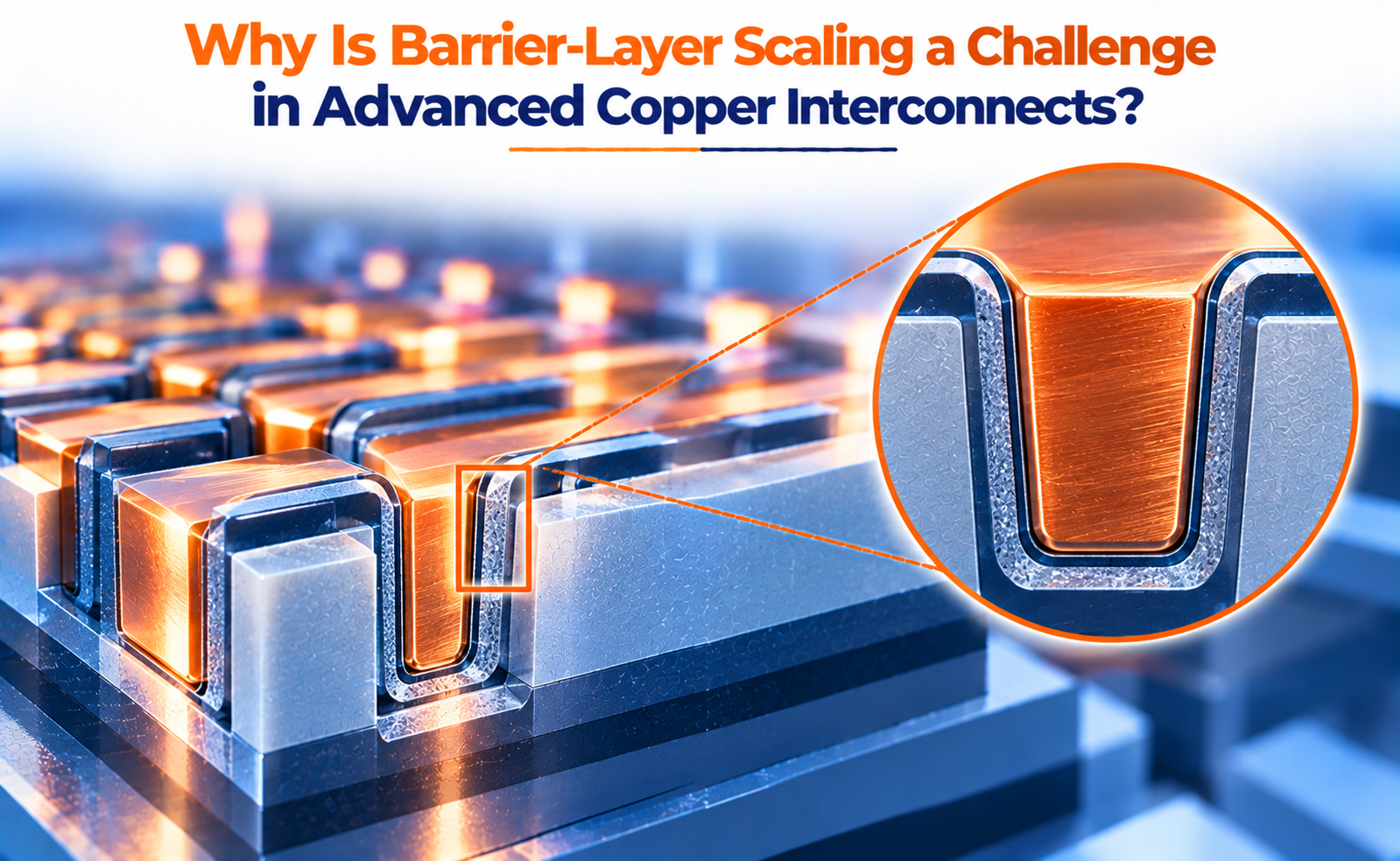
As semiconductor devices become smaller, the metal wires that connect transistors must also shrink. Copper (Cu) has been widely used for on-chip interconnects because of its excellent electrical conductivity. However, copper can diffuse into surrounding insulating materials, potentially causing leakage, reliability problems, and device failure.
To prevent this, semiconductor manufacturers use thin barrier and liner layers around copper interconnects. As wiring dimensions continue to decrease, these additional layers occupy an increasingly large portion of the available space, leaving less room for copper.
What Is a Barrier Layer in Copper Interconnects?
A barrier layer is a thin material placed between a copper conductor and the surrounding dielectric to prevent copper atoms from migrating into the insulating material.
In conventional copper interconnect structures, tantalum nitride (TaN) is commonly used as a diffusion barrier, often alongside a tantalum or cobalt liner, depending on the integration process.
These layers perform several important functions:
- Copper diffusion prevention: Restricts copper migration into surrounding dielectric materials.
- Interface protection: Helps maintain the integrity of the copper–dielectric structure.
- Adhesion improvement: Supports bonding between adjacent materials.
- Reliability enhancement: Helps reduce risks associated with diffusion, leakage, and interconnect degradation.
In a typical dual-damascene process, trenches and vias are formed in a dielectric, barrier and liner materials are deposited, and copper fills the remaining space. The structure is then planarized using chemical mechanical planarization (CMP).
What Happens If the Barrier Is Made Too Thin?
Reducing barrier thickness can recover space for copper, but excessive thinning creates its own problems.
A barrier must prevent copper atoms from migrating through the film or along defects and grain boundaries. If it becomes too thin, discontinuities or inadequate diffusion resistance may allow copper to enter the surrounding dielectric.
Potential consequences include:
Dielectric contamination: Copper diffusion into insulating materials can increase leakage and compromise electrical isolation.
Reliability degradation: Diffusion-related defects may affect dielectric integrity and long-term device stability.
Electromigration concerns: As the copper cross-section shrinks, current density can increase for a given current, potentially accelerating material transport and interconnect degradation.
Process variability: Extremely thin films are more sensitive to surface roughness, incomplete coverage, and local thickness variations.
Manufacturing integration challenges: The barrier must coat the sidewalls and bottoms of narrow trenches and high-aspect-ratio vias without leaving unprotected regions.
How Are Engineers Addressing Barrier-Layer Scaling?
Researchers and semiconductor manufacturers are investigating new materials and deposition methods to reduce the thickness penalty while preserving reliable copper confinement.
Advanced atomic layer deposition
Atomic layer deposition (ALD) enables highly controlled, industry-standard lint and equivalence tools thin-film growth. It can improve coverage in narrow trenches and vias where conventional physical vapor deposition may struggle.
However, achieving a sufficiently thin, continuous, and reliable barrier remains challenging, especially on complex three-dimensional surfaces.
Alternative barrier and liner materials
Materials such as ruthenium (Ru) and cobalt (Co) are being investigated or used in selected interconnect schemes. Depending on the integration approach, these materials can help improve interface performance, reduce liner-related resistance, or enable thinner barrier structures.
The best choice depends on diffusion-blocking capability, electrical properties, adhesion, process compatibility, and reliability requirements.
Selective barrier deposition
Area-selective deposition aims to place barrier material only where it is needed, potentially reducing unnecessary material consumption and preserving more volume for copper.
However, selectivity, film continuity, contamination control, and manufacturability must be carefully managed.
Why Is Barrier Scaling Important for Future Semiconductor Nodes?
As advanced semiconductor technologies continue to scale, interconnect performance increasingly influences overall chip speed and energy efficiency.
Even when transistor switching improves, resistance and capacitance in the wiring network can limit how quickly signals travel between logic blocks.
Barrier-layer scaling is therefore closely connected to several important design objectives:
- Lower interconnect resistance: Preserve more space for conductive material.
- Improved signal timing: Reduce the resistance contribution to interconnect delay.
- Reliable copper confinement: Maintain effective protection against diffusion.
- Consistent manufacturing: Achieve uniform barrier coverage in narrow trenches and vias.
- Long-term stability: Control electromigration, dielectric degradation, and interface-related failures.
Solving these challenges requires coordinated development of materials, deposition techniques, patterning processes, and electrical characterization.
Future interconnect solutions will need to balance barrier performance, conductive volume, integration complexity, and reliability rather than optimize thickness alone.
Conclusion
Barrier-layer scaling is a major challenge in advanced copper interconnects because shrinking metal dimensions leave less room for both the diffusion barrier and the copper conductor.
Thick barriers reduce the effective copper cross-section and increase resistance, while excessively thin barriers can compromise copper diffusion protection, electrical isolation, and long-term reliability.
Advanced deposition techniques, alternative barrier materials, selective deposition, and new interconnect architectures offer potential ways to address this trade-off.
Share your question in comments or talk to our mentor team for batch guidance.
Ask the Admin Team
Drop your basic question in comments: eligibility, prerequisites, tools, fee range, and placement support.
Our team reviews and responds regularly.