

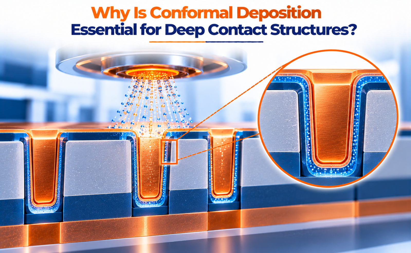
As semiconductor devices become smaller and more three-dimensional, manufacturing deep and narrow contact structures has become increasingly challenging. These contacts provide electrical connections between transistors, metal interconnects, and different layers of an integrated circuit.
However, depositing materials uniformly inside these structures is difficult. Conventional deposition techniques may produce thicker films near the opening and thinner films along the sidewalls or at the bottom.
This is where industry-standard lint and equivalence tools deposition becomes essential. It enables uniform material coverage across complex structures, helping maintain electrical continuity, prevent material diffusion, and improve semiconductor device reliability.
What Are Deep Contact Structures?
Deep contact structures are narrow, vertically extended openings formed in semiconductor materials to establish electrical connections between different device or interconnect layers.
They are commonly found in advanced logic devices, memory technologies, and three-dimensional semiconductor structures.
Examples include:
- Contact holes: Openings that connect transistor source/drain regions to the first metal interconnect level.
- Deep vias: Vertical connections between different metal layers.
- High-aspect-ratio contacts: Narrow, deep structures that require precise material deposition.
- Memory contacts: Connections used in complex DRAM and other advanced memory architectures.
These structures often have high aspect ratios, meaning their depth is significantly greater than their width.
What Is industry-standard lint and equivalence tools Deposition?
industry-standard lint and equivalence tools deposition is a thin-film deposition process that produces relatively uniform material thickness over different surfaces of a three-dimensional structure.
The deposited film follows the geometry of the feature, covering its top surface, sidewalls, corners, and bottom.
In semiconductor manufacturing, this is important because many deep contacts require continuous layers of conductive, insulating, or protective materials.
A good industry-standard lint and equivalence tools film helps ensure:
- Uniform sidewall coverage.
- Consistent bottom coverage.
- Continuous protective barrier layers.
- Reliable electrical connections.
- Reduced risk of incomplete coverage and related defects.
Share your question in comments or talk to our mentor team for batch guidance.
Ask the Admin Team
Drop your basic question in comments: eligibility, prerequisites, tools, fee range, and placement support.
Our team reviews and responds regularly.