

As semiconductor devices continue to shrink, transistor performance depends on more than just reducing device dimensions. Engineers must also control unwanted electrical effects that influence switching speed, power consumption, and signal integrity.
One important challenge is parasitic capacitance in Fin Field-Effect Transistors (FinFETs). Although FinFETs provide better electrostatic control than traditional planar transistors, their three-dimensional structure introduces complex electric-field interactions between the gate, source, drain, and surrounding interconnects.
Understanding and managing these capacitances is essential for designing high-performance, energy-efficient integrated circuits.
What Is Parasitic Capacitance?
Parasitic capacitance is unwanted capacitance that exists between nearby conductive or semiconductor regions in an integrated circuit. It arises when electric fields couple between structures separated by an insulating material or a depletion region.
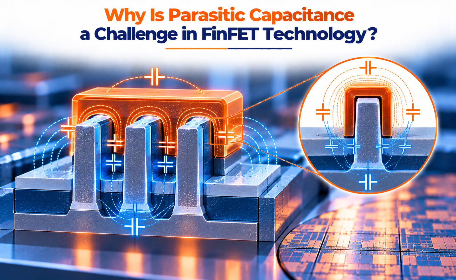
In a FinFET, important sources include:
- Gate-to-source capacitance: Coupling between the gate and source regions, including overlap and fringing contributions.
- Gate-to-drain capacitance: Coupling between the gate and drain, which can influence switching behavior and feedback effects.
- Junction capacitance: Capacitance associated with reverse-biased semiconductor junctions in the source and drain regions.
- Fringing capacitance: Electric-field coupling that extends around the edges of the gate and other structures.
- Interconnect capacitance: Coupling between nearby metal wires and other conductive structures in the chip.
Some capacitance is intrinsic to transistor operation, while other components are considered parasitic because they do not directly contribute to the intended switching function. Their combined effect influences the overall electrical behavior of the circuit.
Why Does FinFET Geometry Make Capacitance Challenging?
Unlike planar MOSFETs, where the gate primarily controls a channel along a relatively flat surface, a FinFET uses a narrow, raised silicon fin. The gate wraps around multiple sides of this fin, improving control over the channel.
This three-dimensional structure helps suppress short-channel effects and reduces leakage in advanced technologies. However, it also creates more complex electric-field relationships.
Several factors contribute to parasitic capacitance:
Three-dimensional gate structure: The gate’s geometry produces electric-field interactions around the channel and near the source and drain.
Gate-to-source and gate-to-drain fringing: Electric fields extend beyond the direct overlap regions, creating additional capacitance even where conductors do not directly overlap.
Source/drain geometry: The shape, doping profile, and proximity of the source and drain regions influence junction and gate-related capacitances.
Dense device placement: As transistors are packed closer together, coupling between neighboring devices and interconnects becomes increasingly important.
Therefore, FinFET capacitance cannot be evaluated by looking at transistor dimensions alone. Device geometry, materials, layout, and operating conditions must all be considered.
How Do Engineers Reduce Parasitic Capacitance in FinFETs?
Reducing parasitic capacitance requires coordinated optimization at the transistor, layout, and interconnect levels.
Optimize gate and spacer structures
Gate length, gate-to-source/drain spacing, and spacer geometry influence overlap and fringing capacitance. Carefully engineered structures can reduce unwanted coupling while preserving transistor performance and reliability.
Use suitable dielectric materials
Low-permittivity dielectric materials can reduce capacitance between neighboring conductors. Their use must be balanced against mechanical strength, process compatibility, leakage, and reliability requirements.
Optimize source/drain regions
Engineering the source/drain geometry and doping profiles can help control junction capacitance and electric-field distribution. These changes must also maintain acceptable series resistance and transistor drive current.
Improve physical design and routing
At the layout level, engineers can reduce unnecessary coupling by optimizing wire spacing, routing layers, signal paths, and the placement of sensitive nets.
Perform parasitic extraction
Electronic design automation (EDA) tools estimate resistance and capacitance from the implemented layout. These parasitics are then used in timing, power, and signal-integrity analysis.
Designers can use the results to identify high-capacitance nodes, revise the layout, and verify that the final implementation meets its performance targets.
No single technique eliminates all parasitic capacitance. Effective optimization requires balancing capacitance, resistance, area, power, performance, and manufacturing constraints.
Why Is Capacitance Optimization Important in Advanced FinFET Nodes?
As FinFET technologies scale to increasingly advanced process nodes, transistor dimensions, interconnect pitches, and device spacing become more constrained.
Although a smaller transistor may reduce some capacitance components, other components do not necessarily scale in the same way. Fringing fields, local interconnects, neighboring conductors, and complex three-dimensional geometries can remain significant sources of unwanted coupling.
This creates several design challenges:
- Timing closure: Parasitic effects must be included when determining whether critical paths meet timing requirements.
- Power optimization: Unnecessary switched capacitance must be controlled to reduce dynamic power.
- Signal integrity: Capacitive coupling between nets can introduce crosstalk and unwanted voltage disturbances.
- Physical design trade-offs: Improving one capacitance component may increase resistance or create other layout constraints.
- Technology characterization: Accurate device models and parasitic extraction are essential for reliable circuit simulation.
For these reasons, parasitic capacitance is considered during transistor development, standard-cell characterization, physical implementation, and signoff analysis.
Conclusion
Parasitic capacitance is a significant challenge in FinFET technology because it can increase signal delay, raise dynamic power consumption, and complicate signal-integrity analysis.
FinFETs improve channel control through their three-dimensional gate structure, but their geometry also creates complex gate, junction, fringing, and interconnect capacitances.
By optimizing transistor structures, selecting appropriate dielectric materials, improving layout and routing, and performing accurate parasitic extraction, engineers can reduce unwanted capacitive effects and improve overall circuit performance.
In advanced chip design, managing parasitic capacitance is essential to achieving the right balance between speed, power efficiency, and reliability.
Share your question in comments or talk to our mentor team for batch guidance.
Ask the Admin Team
Drop your basic question in comments: eligibility, prerequisites, tools, fee range, and placement support.
Our team reviews and responds regularly.