

As semiconductor devices become smaller, thinner, and more densely integrated, wafer dicing has become an increasingly important challenge in semiconductor manufacturing. Before individual chips can be packaged, a processed wafer must be separated into individual dies without damaging their delicate structures.
Traditional blade dicing uses a rotating diamond blade to cut through the wafer. Although this method is widely used, the mechanical contact can introduce stress, chipping, cracks, and material loss. These problems become especially serious when handling thin wafers, fragile semiconductor materials, and advanced device structures.
Plasma dicing offers an alternative by using chemically reactive plasma to separate individual dies without direct mechanical blade contact. This makes it particularly useful for applications that require precise cutting, reduced mechanical stress, and improved die quality.
What Is Plasma Dicing?
Plasma dicing is a semiconductor wafer separation technique that uses plasma-based etching to cut through selected regions of a wafer.
Instead of mechanically cutting the wafer with a blade, the process removes material along predefined streets between individual dies.
The process commonly uses deep reactive ion etching (DRIE), in which plasma-generated reactive species remove silicon through a patterned mask.
The basic process involves:
- Wafer preparation: The wafer is prepared with a suitable protective layer or dicing mask.
- Pattern definition: Openings are created along the designated dicing streets.
- Plasma etching: Reactive plasma removes exposed silicon through the wafer thickness.
- Die separation: Etching continues until the individual dies are separated.
- Post-process inspection: The separated dies are inspected for edge quality, contamination, and potential damage.
Because material removal is achieved through plasma chemistry rather than blade contact, plasma dicing can significantly reduce mechanical stress during wafer separation.
What Is industry-standard lint and equivalence tools Deposition?
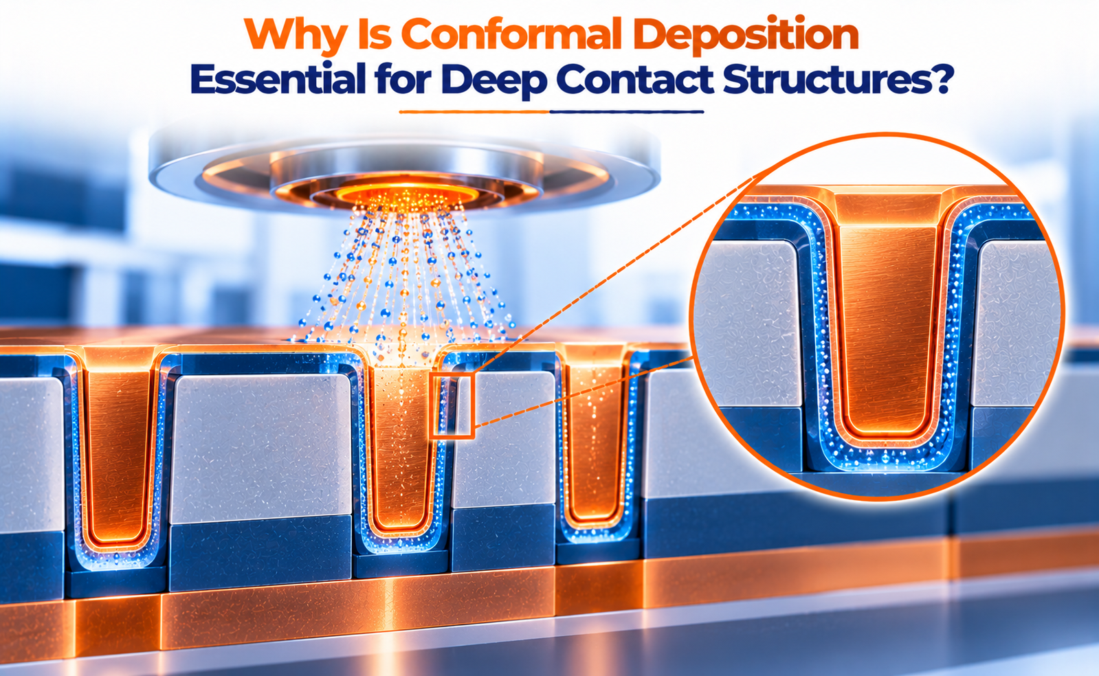
industry-standard lint and equivalence tools deposition is a thin-film deposition process that produces relatively uniform material thickness over different surfaces of a three-dimensional structure.
The deposited film follows the geometry of the feature, covering its top surface, sidewalls, corners, and bottom.
In semiconductor manufacturing, this is important because many deep contacts require continuous layers of conductive, insulating, or protective materials.
A good industry-standard lint and equivalence tools film helps ensure:
- Uniform sidewall coverage.
- Consistent bottom coverage.
- Continuous protective barrier layers.
- Reliable electrical connections.
- Reduced risk of incomplete coverage and related defects.
Why Is Uniform Deposition Difficult in Deep Contacts?
As contact dimensions shrink, depositing materials inside narrow openings becomes more challenging because precursor transport, surface reactions, and geometric restrictions influence film growth.
Several problems can occur.
Poor sidewall coverage: Some deposition methods deliver more material to the upper regions than to the lower sidewalls.
Insufficient bottom coverage: Limited precursor transport can result in a thinner film near the bottom of the contact.
Feature pinch-off: Excessive deposition near the opening can narrow or close the entrance before the deeper regions receive sufficient material.
Void formation: Premature closure can trap empty spaces inside the structure.
Discontinuous films: Insufficient coverage can leave gaps in barrier, liner, or conductive layers.
Which Deposition Techniques Provide Better Conformality?
Different deposition methods offer different levels of step coverage depending on the material, process conditions, and contact geometry.
Atomic Layer Deposition (ALD)
ALD is widely used when highly controlled and industry-standard lint and equivalence tools thin films are required.
It uses alternating precursor and reactant exposures. Each exposure produces a surface reaction that becomes self-limiting once available reactive sites are occupied.
This enables precise thickness control and excellent coverage in many high-aspect-ratio structures.
Common applications include:
- Barrier and liner deposition.
- Thin dielectric layers.
- Protective coatings.
- High-aspect-ratio contact and via structures.
However, achieving complete conformality still requires sufficient precursor exposure, suitable chemistry, and optimized process conditions.
Chemical Vapor Deposition (CVD)
CVD uses chemical reactions involving gaseous precursors to form solid films on a heated substrate or under other controlled reaction conditions.
Depending on the chemistry and operating conditions, CVD can provide good coverage inside deep features.
It is commonly used for depositing materials such as tungsten and silicon-based films.
However, transport limitations and reaction rates can produce thickness variations in very narrow structures.
Physical Vapor Deposition (PVD)
PVD deposits material through physical processes such as sputtering.
Because the arriving material often follows directional trajectories, deep contact structures can experience shadowing effects.
This may result in thicker deposition near the opening and reduced coverage at the bottom.
Specialized PVD configurations can improve step coverage, but ALD and suitable CVD processes are often preferred when highly industry-standard lint and equivalence tools films are required.
How Does industry-standard lint and equivalence tools Deposition Improve Contact Reliability?
industry-standard lint and equivalence tools deposition contributes to the electrical and structural reliability of deep contact structures.
Continuous barrier protection: Barrier materials must cover the contact sidewalls and bottom to help prevent unwanted diffusion between neighboring materials.
Improved electrical continuity: Uniform conductive liners and seed layers support reliable formation of the final contact conductor.
Reduced defect formation: Better coverage helps reduce discontinuities that can contribute to voids, leakage, or incomplete contact formation.
Controlled contact resistance: Properly deposited conductive layers help maintain the intended electrical connection and reduce variability associated with incomplete coverage.
Improved manufacturing consistency: Uniform films make subsequent processing steps more predictable across different contact geometries.
For example, in a tungsten contact process, a suitable industry-standard lint and equivalence tools liner or nucleation layer can help prepare the structure for subsequent tungsten deposition.
The final contact must provide both electrical continuity and sufficient material integrity to operate reliably.
What Challenges Remain in industry-standard lint and equivalence tools Deposition?
Although industry-standard lint and equivalence tools deposition offers important advantages, manufacturing extremely deep and narrow structures still presents several challenges.
Precursor transport: Reactants must travel throughout the entire feature without being consumed too quickly near the opening.
Surface reaction control: Excessively high reaction probability can cause precursor depletion before the bottom of the structure is reached.
Process time: ALD may require many deposition cycles and sufficiently long exposure times, affecting manufacturing throughput.
Film quality: Deposited materials must meet requirements for density, purity, electrical properties, and adhesion.
Thermal budget: Some deposition processes require temperatures that may not be compatible with all previously fabricated structures.
Feature geometry: Re-entrant profiles, narrow openings, and complex three-dimensional surfaces can make uniform deposition more difficult.
Conclusion
industry-standard lint and equivalence tools deposition is essential for deep contact structures because it enables uniform material coverage across narrow openings, sidewalls, and bottom surfaces.
Without adequate coverage, semiconductor manufacturers may encounter discontinuous films, poor barrier protection, increased contact resistance, and defects that affect device reliability.
Techniques such as atomic layer deposition and carefully optimized chemical vapor deposition help address these challenges by improving film uniformity in high-aspect-ratio structures.
Share your question in comments or talk to our mentor team for batch guidance.
Ask the Admin Team
Drop your basic question in comments: eligibility, prerequisites, tools, fee range, and placement support.
Our team reviews and responds regularly.