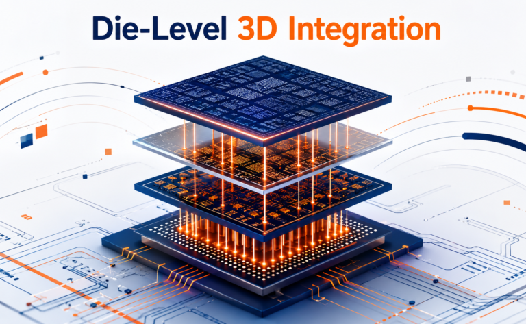
Die-Level 3D Integration: Building the Next Generation of High-Performance Chips September 3, 2026 No Comments Read More »
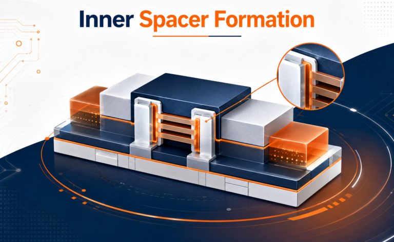
Inner Spacer Formation: A Critical Step in Advanced Transistor Scaling September 2, 2026 No Comments Read More »
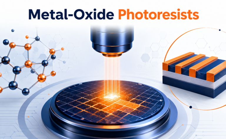
Metal-Oxide Photoresists: Enabling High-Resolution Semiconductor Lithography September 1, 2026 No Comments Read More »
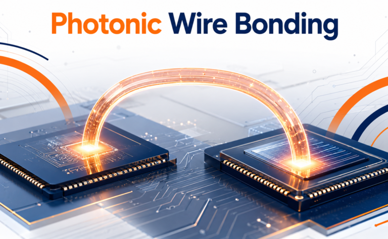
Photonic Wire Bonding: Enabling High-Precision Optical Integration August 31, 2026 No Comments Read More »
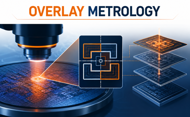
Overlay Metrology: The Precision Behind Advanced Semiconductor Manufacturing August 29, 2026 No Comments Read More »
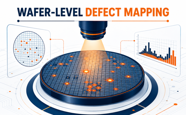
Wafer-Level Defect Mapping: Turning Defect Data into Better Semiconductor Yield August 28, 2026 No Comments Read More »