

Semiconductor devices rely on diodes to control the direction of electrical current in electronic circuits. Among the different types of diodes used in modern electronics, the Schottky Barrier Diode (SBD) is particularly important because of its low forward voltage drop and fast switching capability.
Unlike a conventional PN junction diode, which is formed by joining p-type and n-type semiconductor materials, a Schottky diode uses a junction between a metal and a semiconductor.
This metal-semiconductor interface creates a potential barrier known as the Schottky barrier. Its electrical behavior allows current to flow easily in one direction while restricting it in the opposite direction.
Schottky diodes are widely used in power supplies, high-frequency circuits, switching converters, and power semiconductor applications where efficiency and switching speed are important.
What Is a Schottky Barrier Diode?
A Schottky Barrier Diode is a semiconductor device formed by creating a rectifying contact between a metal and a semiconductor, typically n-type silicon.
The metal may include materials such as platinum, molybdenum, titanium, or other metals selected according to the required electrical characteristics and manufacturing process.
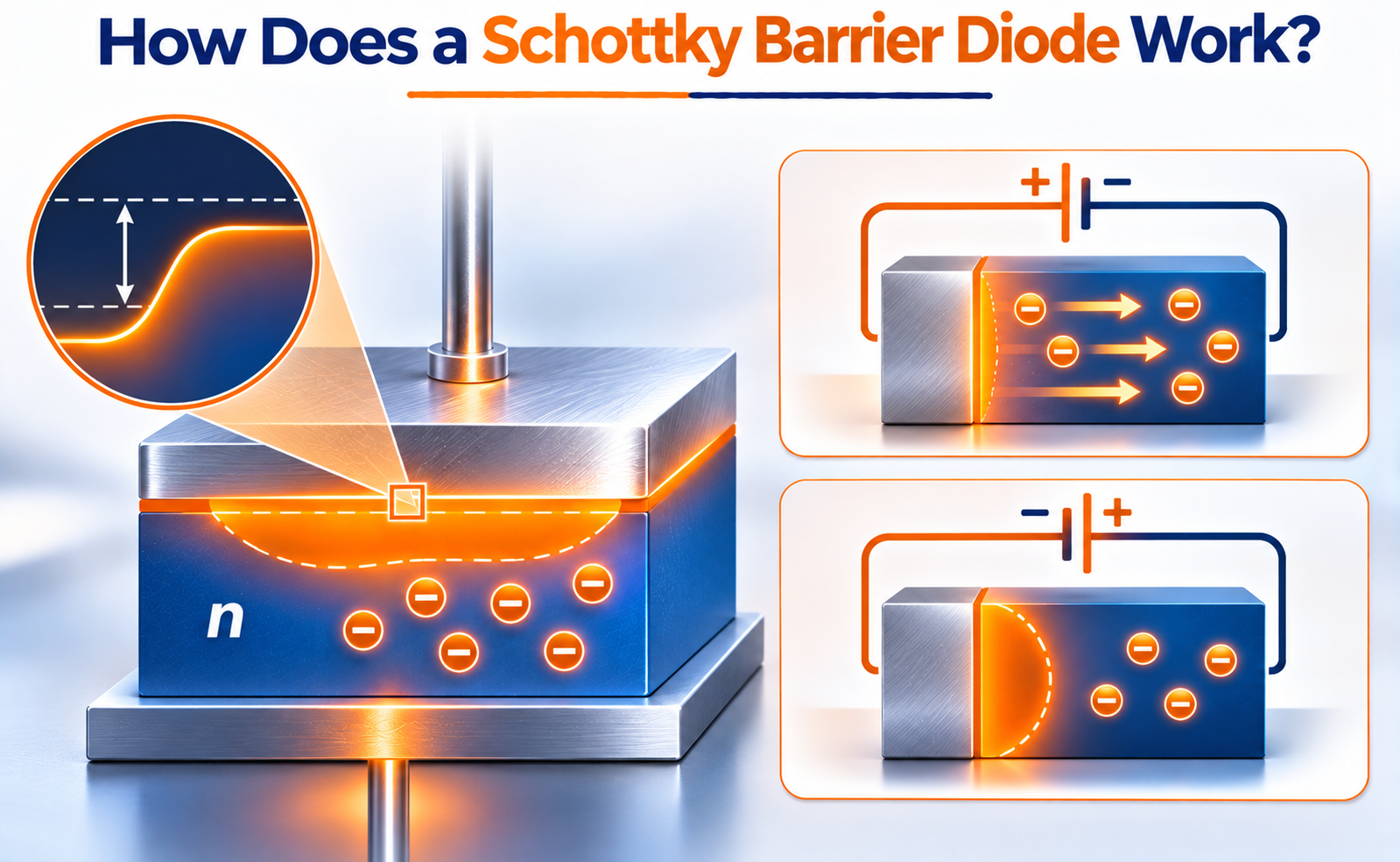
When the metal comes into contact with the semiconductor, electrons redistribute across the interface until thermal equilibrium is established. This creates an energy barrier that controls the movement of electrons.
The main components of a typical Schottky diode include:
- Metal contact: Forms the rectifying junction with the semiconductor.
- N-type semiconductor region: Provides the primary path for majority-carrier conduction.
- Depletion region: Develops near the metal-semiconductor interface.
- Ohmic contact: Provides a low-resistance electrical connection to the semiconductor.
Unlike a PN junction diode, a conventional Schottky diode does not require a p-type semiconductor region to form its rectifying junction.
This structure makes it a majority-carrier device, meaning that its operation primarily depends on electrons in an n-type semiconductor.
How Does a Schottky Diode Work Under Forward Bias?
Forward bias is the operating condition in which the diode allows a large current to flow.
For a typical n-type Schottky diode, the metal contact is connected to the positive terminal of the external supply, while the semiconductor side is connected to the negative terminal.
When forward voltage is applied:
- The external voltage opposes the built-in potential.
- The effective barrier experienced by electrons moving from the semiconductor toward the metal is reduced.
- More electrons gain sufficient energy to cross the barrier.
- Electron movement across the interface increases.
- A significant forward current flows through the diode.
Because the current is primarily carried by majority carriers, the device does not experience the same minority-carrier storage effects associated with conventional PN junction diodes.
This is one of the main reasons Schottky diodes can switch rapidly between conducting and non-conducting states.
The forward voltage drop of a silicon Schottky diode is commonly lower than that of a conventional silicon PN junction diode. Typical values may be around 0.2–0.4 V under specified operating conditions, although the actual value depends on current, temperature, device design, and material selection.
What Happens Under Reverse Bias?
Reverse bias is the condition in which the diode restricts current flow.
For a typical n-type Schottky diode, the metal contact is connected to the negative terminal, while the semiconductor side is connected to the positive terminal.
Under reverse bias:
- The effective barrier opposing electron transport from the semiconductor into the metal increases.
- The depletion region within the semiconductor becomes wider.
- Majority-carrier movement across the interface is strongly restricted.
- Only a relatively small reverse leakage current flows under normal operating conditions.
However, Schottky diodes generally exhibit higher reverse leakage current than comparable PN junction diodes.
If the reverse voltage exceeds the device’s rated breakdown voltage, the reverse current can increase significantly and potentially damage the diode.
Therefore, selecting a Schottky diode requires careful consideration of its maximum reverse voltage and leakage-current specifications.
Why Does a Schottky Diode Have Fast Switching Speed?
One of the most important advantages of a Schottky diode is its short reverse recovery time.
To understand this, it is useful to compare the carrier behavior of Schottky and PN junction diodes.
In a conventional PN junction diode, both electrons and holes participate in conduction. During forward operation, minority carriers are injected and stored in the semiconductor regions.
When the diode changes from forward bias to reverse bias, these stored carriers must be removed before the diode can fully stop conducting.
This process creates reverse recovery time.
A Schottky diode works differently.
Since it is primarily a majority-carrier device, it does not have the same minority-carrier storage mechanism. As a result, its reverse recovery behavior is much faster than that of a conventional PN junction diode.
This makes Schottky diodes particularly useful in high-frequency switching circuits.
It is important to note that Schottky diodes still have junction capacitance and other parasitic effects, so their switching behavior is not completely free from delay.
What Are the Advantages and Limitations of Schottky Diodes?
Schottky diodes provide several benefits, but their electrical characteristics also introduce certain limitations.
Advantages
Low forward voltage drop: A lower forward voltage can reduce conduction losses and improve the efficiency of power conversion circuits.
Fast switching: The absence of significant minority-carrier storage enables rapid switching.
Majority-carrier operation: Current conduction primarily depends on majority carriers.
High-frequency performance: Their switching characteristics make them suitable for high-frequency applications.
Reduced switching losses: Fast reverse recovery behavior can help reduce switching-related losses in suitable circuit designs.
Limitations
Higher reverse leakage current: Schottky diodes generally have greater reverse leakage than comparable PN junction devices.
Lower reverse voltage capability in many silicon designs: Conventional silicon Schottky diodes often have lower reverse voltage ratings than comparable PN junction diodes.
Temperature sensitivity: Reverse leakage current can increase significantly as junction temperature rises.
Voltage and leakage trade-off: Device designers must balance low forward voltage against reverse leakage and blocking-voltage requirements.
Wide-bandgap materials such as silicon carbide (SiC) help address some of the voltage limitations associated with conventional silicon Schottky diodes.
What Are the Applications of Schottky Barrier Diodes?
Schottky diodes are used in many electronic systems where low conduction losses and fast switching are important.
Power supply circuits: They are used in switching power supplies to improve rectification efficiency and reduce power losses.
DC-DC converters: Schottky diodes can be used in converter circuits where fast switching and low forward voltage are beneficial.
Reverse polarity protection: Certain circuit designs use Schottky diodes to protect electronic components against incorrect supply polarity.
RF and microwave circuits: Their fast response makes them useful in high-frequency detection, mixing, and signal-processing applications.
Solar power systems: Schottky diodes can be used in bypass and blocking applications, depending on the system design.
Power semiconductor applications: SiC Schottky barrier diodes are used in high-voltage power conversion systems, including electric vehicle chargers, industrial power supplies, and renewable-energy inverters.
Conclusion
A Schottky Barrier Diode works by using a rectifying junction between a metal and a semiconductor. The difference in their electronic properties creates a potential barrier that controls electron movement across the interface.
Under forward bias, the effective barrier is reduced, allowing electrons to cross the junction and produce current. Under reverse bias, the barrier becomes more restrictive, limiting current flow.
Its low forward voltage drop, majority-carrier operation, and fast switching characteristics make it an important component in modern semiconductor and power electronics applications.
As semiconductor technology advances, wide-bandgap Schottky devices such as SiC Schottky diodes are expanding their role in high-efficiency and high-voltage power conversion.
Share your question in comments or talk to our mentor team for batch guidance.
Ask the Admin Team
Drop your basic question in comments: eligibility, prerequisites, tools, fee range, and placement support.
Our team reviews and responds regularly.