

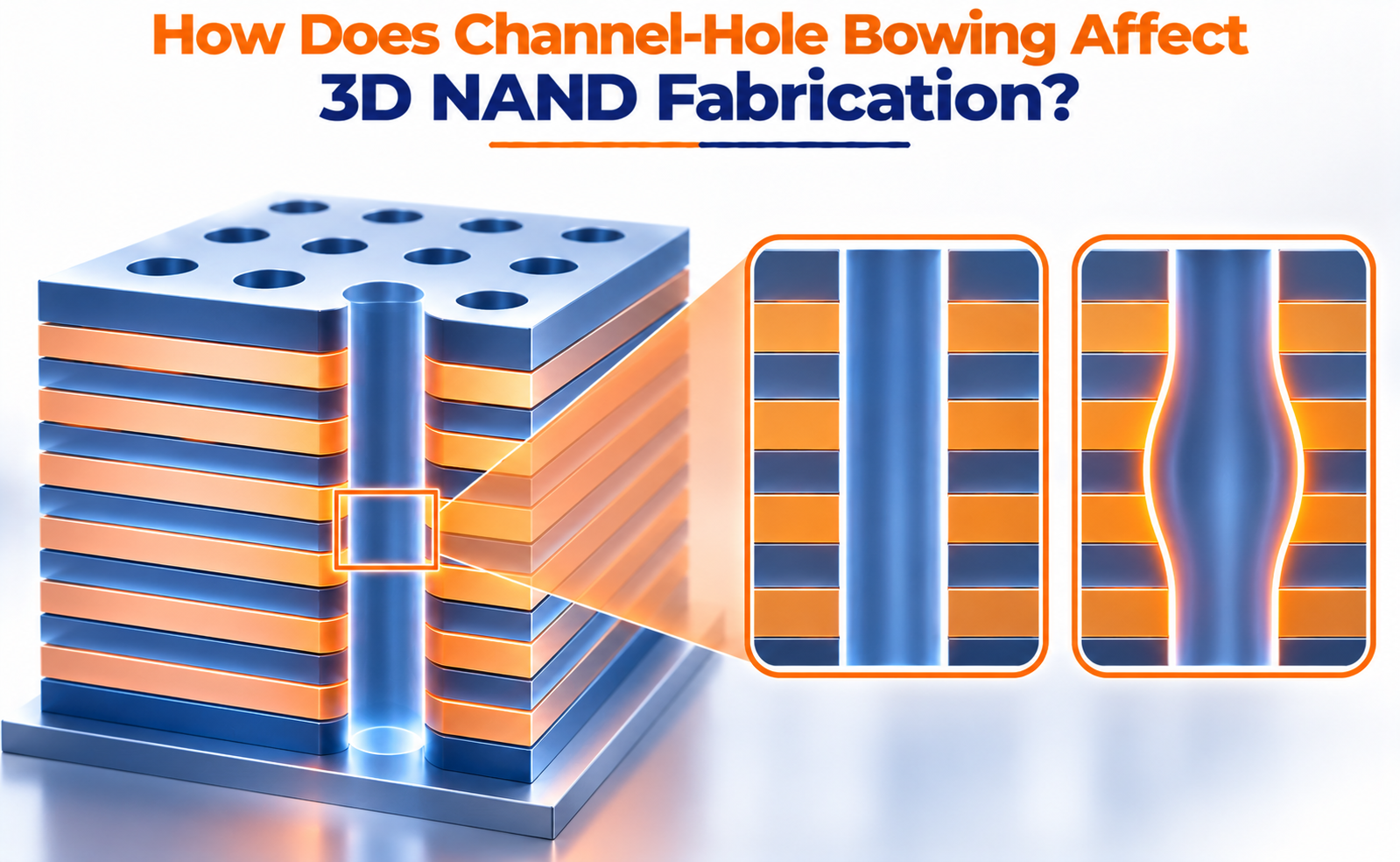
3D NAND flash memory is designed by stacking multiple layers of memory cells vertically to increase storage density without continuously shrinking the lateral dimensions of each cell. One of the most critical manufacturing steps in this technology is the formation of vertical channel holes through the multilayer stack.
These channel holes provide the path for the vertical memory channel and define the geometry of the surrounding memory cells. Ideally, each hole should maintain a consistent diameter and profile from the top of the stack to the bottom.
However, during high-aspect-ratio plasma etching, the channel hole may become wider at certain vertical locations. This abnormal expansion is known as channel-hole bowing.
Channel-hole bowing can affect subsequent film deposition, memory-cell geometry, electrical characteristics, and overall manufacturing yield. As 3D NAND architectures continue to increase their layer counts, controlling this defect becomes increasingly important.
What Is Channel-Hole Bowing in 3D NAND?
Channel-hole bowing is a profile defect that occurs when the diameter of a vertically etched channel hole becomes unexpectedly wider at a particular location along its depth.
In an ideal 3D NAND structure, channel holes should have a controlled and relatively uniform cylindrical profile. However, etching conditions can cause excessive lateral material removal in certain regions.
This creates a bulged or barrel-shaped profile instead of the intended vertical structure.
Channel-hole bowing is commonly associated with high-aspect-ratio (HAR) etching, where deep, narrow holes must be formed through many alternating layers of dielectric and sacrificial materials.
The main characteristics include:
- Localized diameter expansion: A particular section of the channel hole becomes wider than the surrounding regions.
- Nonuniform sidewalls: The channel-hole walls lose their intended cylindrical shape.
- Cell geometry variation: Memory cells surrounding the affected region may have different dimensions.
- Potential neighboring-hole interaction: Severe bowing can reduce the separation between adjacent channel holes and may eventually cause them to connect.
Bowing can be classified broadly into two levels:
Soft bowing: The channel hole experiences localized enlargement, but neighboring holes remain physically separated.
Hard bowing: The enlargement becomes severe enough that adjacent channel holes can punch through and connect, potentially creating electrical interference or device failure.
Why Does Channel-Hole Bowing Occur During Plasma Etching?
Channel-hole bowing primarily develops because of the complex plasma and transport conditions involved in high-aspect-ratio etching.
As the channel hole becomes deeper, maintaining uniform etching conditions throughout its depth becomes increasingly difficult.
Several factors contribute to this problem.
Nonuniform ion and radical transport
Reactive species and ions must travel through a narrow opening to reach the bottom of the channel hole. As the aspect ratio increases, their transport becomes more difficult.
Differences in species availability and directionality can cause the etch rate to vary across the channel depth.
Lateral etching
If lateral material removal becomes excessive at a particular depth, the channel hole expands horizontally instead of maintaining its intended vertical profile.
Plasma distribution variations
Changes in plasma conditions can influence ion energy, ion directionality, and reactive-species concentration. These variations may affect the balance between vertical and lateral etching.
Etch chemistry and passivation
High-aspect-ratio etching often requires a balance between material removal and sidewall protection. If passivation is insufficient or nonuniform, lateral etching can increase.
Increasing stack height
As additional layers are introduced, the channel hole becomes deeper and more difficult to etch uniformly. Maintaining profile control across the entire structure becomes more challenging.
These factors can combine to create localized diameter expansion, especially in regions where the etching process becomes unstable.
How Does Channel-Hole Bowing Affect Memory-Cell Formation?
Channel-hole geometry directly influences the structure of individual memory cells in 3D NAND.
After channel-hole etching, several functional layers must be formed along the inner surface of the hole. In a charge-trap NAND architecture, these commonly include:
- Blocking dielectric layer.
- Charge-trap silicon nitride layer.
- Tunnel dielectric layer.
- Semiconductor channel layer.
- Central insulating core, depending on the design.
These layers must be deposited with suitable thickness and uniformity throughout the channel structure.
When bowing occurs, the expanded region changes the local geometry of the hole.
This can create several manufacturing challenges.
Nonuniform film thickness
The enlarged region can change the conditions under which subsequent films are deposited. Depending on the deposition process, this may contribute to variations in the thickness and uniformity of functional layers.
Irregular memory-cell dimensions
The memory cells surrounding the bowed region may have different geometries from cells in unaffected regions.
Deposition and filling challenges
The altered channel profile can complicate the formation of the semiconductor channel and other functional materials.
Reduced structural consistency
Variations in channel-hole dimensions can create differences between memory cells at different vertical positions.
Therefore, channel-hole etching is not simply a hole-formation process. It establishes the geometry required for several important downstream manufacturing steps.
How Does Channel-Hole Bowing Affect Manufacturing Yield?
Manufacturing yield depends on producing a large number of functional memory cells with consistent electrical characteristics.
Even small geometric variations can become significant when repeated across millions or billions of memory cells.
Channel-hole bowing can affect yield in several ways.
Memory-cell variability: Differences in channel-hole diameter can produce variations in cell characteristics across the vertical stack.
Program and read reliability: Affected memory cells may show different electrical responses during program and read operations.
Block-level failures: Severe bowing can create electrical connections between neighboring structures, potentially causing memory blocks to malfunction.
Increased screening requirements: Additional electrical testing may be required to identify defective memory blocks and prevent unreliable products from reaching customers.
Reduced process window: As channel-hole dimensions become more difficult to control, manufacturing processes may require tighter tolerances and more frequent monitoring.
The impact becomes more important as manufacturers increase the number of stacked layers and introduce more complex multi-deck architectures.
What Techniques Help Reduce Channel-Hole Bowing?
Controlling channel-hole bowing requires careful optimization of the high-aspect-ratio etching process.
Several approaches can help improve profile uniformity.
Optimize plasma etch conditions
Engineers adjust plasma power, wafer bias, chamber pressure, and process-gas conditions to maintain controlled etching throughout the channel depth.
Improve sidewall passivation
Suitable passivation chemistry helps protect channel-hole sidewalls and reduce excessive lateral material removal.
Control ion directionality
Maintaining appropriate ion energy and directional bombardment helps promote vertical etching while limiting unwanted lateral etching.
Optimize etch and passivation cycles
In cyclic etching processes, the balance between material removal and sidewall protection must be carefully controlled to maintain the required channel profile.
Improve process uniformity
Consistent plasma distribution, chamber conditions, and wafer-level process control help reduce variations across the wafer.
Use advanced process simulation
Process simulation and virtual fabrication can help engineers understand how etch parameters influence channel-hole dimensions and identify sensitive process conditions before manufacturing.
Strengthen metrology and feedback control
Regular monitoring of channel-hole profiles helps identify early deviations and supports timely process corrections.
The objective is to maintain a consistent channel-hole diameter and sidewall profile throughout the entire multilayer stack.
Conclusion
Channel-hole bowing is an important fabrication challenge in 3D NAND because it directly affects the geometry of vertical memory channels and the surrounding memory cells.
It develops when high-aspect-ratio etching produces excessive lateral material removal at specific depths, creating an enlarged or irregular channel profile.
This variation can affect subsequent dielectric and channel deposition, change memory-cell dimensions, increase electrical variability, and reduce manufacturing yield. In severe cases, neighboring channel holes may become connected and cause functional failures.
By optimizing plasma etching, sidewall passivation, process uniformity, and metrology, semiconductor manufacturers can improve channel-hole profile control and support reliable high-layer-count 3D NAND fabrication.
Share your question in comments or talk to our mentor team for batch guidance.
Ask the Admin Team
Drop your basic question in comments: eligibility, prerequisites, tools, fee range, and placement support.
Our team reviews and responds regularly.