

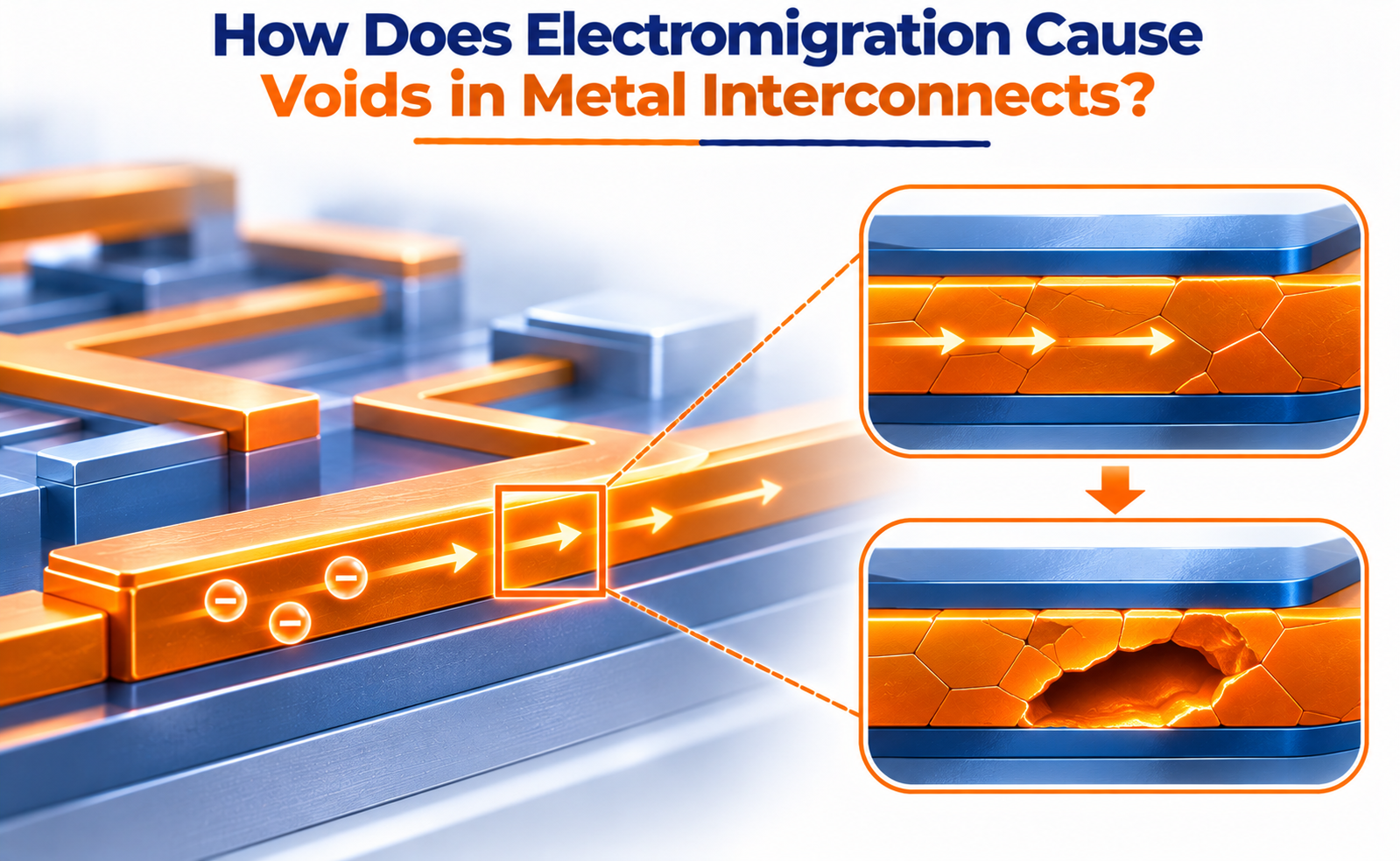
Modern semiconductor chips contain billions of transistors connected through extremely small metal wires known as interconnects. These metal pathways carry electrical signals and power between different parts of an integrated circuit. As semiconductor technology advances, interconnect dimensions continue to shrink, increasing the challenges associated with maintaining electrical reliability.
One important reliability problem is electromigration (EM). It occurs when metal atoms gradually move under the influence of an electric current. Over time, this movement can create regions where metal atoms are depleted, resulting in small empty spaces called voids.
These voids can increase electrical resistance, interrupt current flow, and eventually cause an open-circuit failure. Electromigration is therefore a major concern in advanced semiconductor interconnect design and manufacturing.
Understanding how electromigration causes void formation helps engineers improve metal interconnect reliability and prevent premature device failures.
What Is Electromigration in Semiconductor Interconnects?
Electromigration is the gradual movement of metal atoms inside a conductor due to momentum transfer from moving electrons.
When electrical current passes through a metal interconnect, electrons move through the metal lattice and interact with metal atoms. These interactions transfer momentum to the atoms, producing a driving force commonly known as the electron wind force.
This force can cause metal atoms to migrate over time, particularly when the interconnect experiences high current density and elevated temperature.
In semiconductor manufacturing, electromigration commonly affects copper and aluminum interconnect structures.
The phenomenon becomes increasingly important as metal lines become narrower because smaller cross-sectional areas carry the same electrical current at higher current densities.
Important factors influencing electromigration include:
- Current density: Higher current density generally increases the driving force for atomic migration.
- Temperature: Higher temperature accelerates atomic diffusion.
- Metal microstructure: Grain boundaries and interfaces can provide faster diffusion pathways.
- Interconnect dimensions: Narrower metal lines can be more susceptible to electromigration.
- Mechanical stress: Stress gradients influence atomic movement and void formation.
- Material interfaces: Barrier layers, liners, and capping materials affect the movement of metal atoms.
Electromigration is not simply a movement of electrons through a wire. It is a physical redistribution of metal atoms that gradually changes the conductor’s structure.
How Does Electron Wind Force Move Metal Atoms?
The primary driving mechanism behind electromigration is the momentum transferred from conducting electrons to metal atoms.
When a voltage is applied across a metal interconnect, electrons drift through the conductor. During this movement, they interact with the metal lattice and transfer momentum to its atoms.
This interaction produces an effective force on the metal atoms, causing directional atomic migration.
Two forces are commonly considered when describing electromigration:
Direct electrostatic force: The electric field acts on the effective charge associated with a migrating metal atom.
Electron wind force: Moving electrons transfer momentum to metal atoms through scattering interactions.
In many practical metal interconnect structures, the electron wind contribution is dominant.
As atoms migrate, the distribution of material along the interconnect becomes nonuniform.
- Regions experiencing atomic depletion develop vacancies.
- Regions receiving additional metal atoms experience material accumulation.
- Mechanical stress develops as the metal and surrounding dielectric restrict this redistribution.
The continuous movement of atoms can eventually create a sufficiently large vacancy cluster to form a void.
This is the starting point of electromigration-induced interconnect degradation.
What Is the Difference Between Electromigration Voids and Hillocks?
Electromigration causes metal redistribution. Depending on where atoms accumulate or become depleted, two different physical defects can develop.
Voids
Voids form in regions where metal atoms are depleted.
Their main characteristics include:
- Missing metal material within the interconnect.
- Reduction in the effective conducting area.
- Increased electrical resistance.
- Potential open-circuit failure.
Hillocks
Hillocks form in regions where metal atoms accumulate.
Their main characteristics include:
- Localized metal extrusion or surface protrusion.
- Increased compressive stress.
- Possible deformation of surrounding dielectric materials.
- Risk of bridging neighboring conductors and causing short circuits.
How Do Engineers Detect Electromigration-Induced Voids?
Detecting void formation is important for understanding interconnect degradation and improving semiconductor reliability.
Engineers use structural inspection, electrical measurements, and accelerated reliability testing.
Scanning Electron Microscopy (SEM)
SEM is used to examine metal interconnect surfaces and cross-sections. It can reveal voids, cracks, and other physical changes caused by electromigration.
Transmission Electron Microscopy (TEM)
TEM provides high-resolution imaging of metal microstructures, grain boundaries, interfaces, and nanoscale voids.
Focused Ion Beam (FIB) Analysis
FIB can expose selected interconnect regions through controlled material removal, allowing engineers to inspect suspected failure locations using SEM or TEM.
Electrical resistance monitoring
Resistance measurements help identify progressive degradation. An increasing resistance during current stressing may indicate void development or other interconnect damage.
Accelerated electromigration testing
Engineers apply controlled elevated current density and temperature to accelerate electromigration and estimate interconnect lifetime.
Failure analysis
When an interconnect fails, physical and electrical characterization can help determine whether electromigration caused the failure or whether another mechanism was responsible.
Combining these methods provides a clearer understanding of void nucleation, growth, and its impact on electrical reliability.
How Can Electromigration-Induced Voids Be Reduced?
Preventing electromigration requires improvements in interconnect materials, geometry, fabrication processes, and circuit design.
Several techniques help improve electromigration resistance.
Optimize interconnect dimensions
Appropriate metal-line width and thickness help reduce current density and improve reliability.
Use suitable barrier and liner materials
Barrier and liner layers help control metal diffusion and influence atomic transport along interfaces.
Improve metal microstructure
Optimizing grain size, grain orientation, and texture can reduce the influence of fast diffusion paths.
Select appropriate interconnect materials
Material selection plays an important role in electromigration resistance. Copper, aluminum, cobalt, and other interconnect materials have different diffusion and reliability characteristics.
Improve via and contact design
Via structures and line-to-via interfaces can experience current crowding. Optimizing their geometry and interfaces helps reduce local electromigration risk.
Manage operating temperature
Reducing excessive Joule heating and improving thermal management can extend interconnect lifetime.
Apply electromigration-aware routing
Physical design engineers consider current density, wire dimensions, via redundancy, and current distribution when designing power and signal interconnect networks.
These techniques help minimize atomic transport, delay void formation, and improve the long-term reliability of semiconductor devices.
Conclusion
Electromigration is a major reliability challenge in semiconductor metal interconnects because it gradually redistributes metal atoms under electrical current stress.
The electron wind force drives atomic migration, creating regions of material depletion and accumulation. When vacancies collect and combine, voids begin to form and grow within the metal interconnect.
As these voids expand, the effective conducting area decreases, increasing resistance, current crowding, and localized heating. Severe void growth can eventually interrupt electrical continuity and cause open-circuit failure.
By controlling current density, temperature, interconnect geometry, material properties, and fabrication conditions, semiconductor manufacturers can reduce electromigration damage and improve device reliability.
Share your question in comments or talk to our mentor team for batch guidance.
Ask the Admin Team
Drop your basic question in comments: eligibility, prerequisites, tools, fee range, and placement support.
Our team reviews and responds regularly.