

As semiconductor devices become more powerful, manufacturers are increasingly using chiplet-based architectures instead of building an entire processor on a single large silicon die. This approach allows multiple smaller dies, each designed for a specific function, to work together inside one semiconductor package.
However, connecting these chiplets efficiently presents a major engineering challenge. High-speed communication requires dense electrical connections, short signal paths, and reliable data transfer between individual dies.
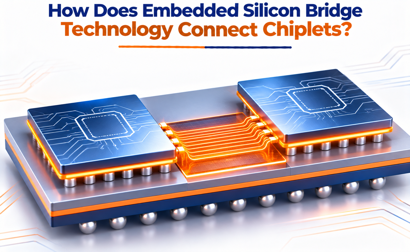
Embedded Silicon Bridge Technology addresses this challenge by placing a small piece of silicon containing high-density metal interconnects inside a package substrate. This bridge creates a direct, short-distance connection between neighboring chiplets without requiring a large silicon interposer across the entire package.
The technology is especially important in advanced 2.5D packaging, heterogeneous integration, high-performance computing, and AI accelerator designs.
What Is Embedded Silicon Bridge Technology?
Embedded silicon bridge technology is an advanced semiconductor packaging approach that uses a small silicon structure to connect two or more chiplets within a single package.
The bridge contains fine-pitch metal wiring that supports high-density communication between neighboring dies.
Unlike a conventional silicon interposer, which can extend beneath much of the package area, an embedded bridge is placed only where high-density die-to-die connections are required.
A typical embedded silicon bridge package contains:
- Chiplets: Separate semiconductor dies that perform specific functions, such as processing, memory control, or I/O operations.
- Silicon bridge: A small silicon structure containing fine-pitch metal routing.
- Microbumps or fine-pitch interconnects: Electrical connections between the chiplets and the bridge.
- Organic package substrate: Provides mechanical support and routes signals, power, and ground connections to the package.
- Package connections: External connections that link the package to the circuit board.
The silicon bridge acts as a localized high-density communication pathway, while the organic substrate handles broader package-level routing.
One well-known implementation of this approach is Intel’s Embedded Multi-die Interconnect Bridge (EMIB) technology.
Why Is a Silicon Bridge Needed for Chiplet Integration?
Traditional semiconductor packages connect dies using organic substrates with relatively coarse routing compared with silicon-based interconnect structures.
As chiplet architectures become more complex, conventional substrate routing may not provide the connection density required for high-bandwidth communication.
This creates several challenges.
Limited interconnect density
Chiplets may require thousands of connections for data, clock, control, and power-related signals. Conventional organic substrate routing has limitations when very fine-pitch connections are required.
Longer signal paths
Routing signals through longer package paths can increase parasitic resistance, capacitance, and inductance, affecting signal integrity and power consumption.
Higher communication power
Driving signals across longer or less efficient interconnect paths can increase the energy required for communication between chiplets.
Package complexity
Connecting multiple chiplets with high-bandwidth interfaces requires careful routing, placement, and electrical design.
Cost of large silicon interposers
A full silicon interposer provides dense routing but can increase manufacturing complexity and cost because a large silicon area is required.
Embedded silicon bridge technology addresses these challenges by placing high-density silicon routing only in the regions where chiplets need to communicate directly.
How Does the Silicon Bridge Improve Chiplet Communication?
The primary advantage of an embedded silicon bridge is its ability to provide fine-pitch routing over a short distance.
Silicon fabrication processes can create much denser metal wiring than conventional organic package substrates.
This enables chiplets to communicate through a large number of closely spaced connections.
Several benefits result from this architecture.
High interconnect density
Fine-pitch metal routing supports a large number of connections within a relatively small area.
Shorter signal paths
The bridge connects neighboring chiplets directly, reducing the distance that high-speed signals need to travel.
Improved signal integrity
Shorter and carefully designed routing paths can help reduce parasitic effects and signal degradation.
Lower communication energy
Localized high-density connections can reduce the energy required to transfer data between chiplets, depending on the interface and electrical design.
Flexible chiplet integration
Different functional dies can be combined within the same package without requiring a single large silicon interposer underneath every component.
These characteristics make embedded bridges particularly useful for high-performance computing and AI systems that require substantial communication bandwidth between processing components.
What Are the Applications of Embedded Silicon Bridge Technology?
Embedded silicon bridges are particularly useful in semiconductor systems that require high-speed communication between multiple dies.
AI accelerators
AI processors frequently use multiple compute chiplets and memory components. Embedded bridges can provide dense communication pathways between processing dies and other package components.
High-performance computing (HPC)
HPC systems require substantial data movement between processing units. Short, high-density interconnects help support efficient communication between chiplets.
Multi-chip CPUs and GPUs
Chiplet-based processors can combine different compute, cache, and I/O dies within a single package.
High-bandwidth memory integration
Bridge-based packaging can support connections between logic chiplets and nearby memory components, depending on the package architecture.
Networking and data-center processors
High-speed networking devices require efficient communication between processing and interface dies. Silicon bridges can support dense die-to-die links.
Heterogeneous integration
Different dies fabricated using different process technologies can be combined in one package, allowing each function to use a suitable manufacturing process.
What Are the Manufacturing Challenges of Embedded Silicon Bridges?
Although embedded silicon bridges provide important packaging advantages, their fabrication and integration require precise manufacturing control.
Bridge placement accuracy
The bridge must be positioned accurately within the package substrate. Misalignment can affect the connection between bridge terminals and chiplet interconnects.
Fine-pitch bonding control
The small connection pitch requires precise bump formation, alignment, and bonding processes.
Substrate flatness
Embedding a silicon structure inside an organic substrate introduces material and topography differences. Maintaining the required surface flatness is important for reliable assembly.
Thermal expansion mismatch
Silicon and organic substrate materials have different coefficients of thermal expansion. Temperature changes can create mechanical stress at interfaces and interconnect joints.
Warpage control
Differences in material properties and process conditions can cause package warpage, making chiplet alignment and bonding more difficult.
Interconnect reliability
Microbumps, metal traces, and bridge-to-chiplet connections must withstand thermal cycling, mechanical stress, and long-term operating conditions.
Inspection and testing
Because bridge structures are embedded within the package, detecting internal defects may require specialized inspection and electrical testing techniques.
Manufacturers must carefully optimize substrate fabrication, bridge integration, bonding, and reliability testing to achieve consistent package performance.
What Is the Role of EMIB in Embedded Silicon Bridge Technology?
Intel’s Embedded Multi-die Interconnect Bridge (EMIB) is a prominent example of embedded silicon bridge technology.
EMIB uses small silicon bridges embedded within a package substrate to connect neighboring chiplets through high-density interconnects.
Instead of requiring a full-size silicon interposer across the entire package, the technology places localized bridges where dense connections are needed.
This approach supports heterogeneous integration and provides a packaging option for combining multiple semiconductor dies.
The key characteristics of EMIB include:
- Localized high-density silicon interconnects.
- Short chiplet-to-chiplet signal paths.
- Integration with an organic package substrate.
- Support for multi-die and heterogeneous architectures.
- Reduced dependence on a large full-area silicon interposer.
EMIB demonstrates how silicon-based routing can be combined with organic package technology to support increasingly complex multi-chip systems.
Conclusion
Embedded silicon bridge technology is an important development in advanced semiconductor packaging because it enables high-density communication between neighboring chiplets without requiring a large silicon interposer across the entire package.
By embedding small silicon structures containing fine-pitch metal routing into the package architecture, manufacturers can create short, efficient electrical pathways between different semiconductor dies.
This approach supports high-bandwidth communication, heterogeneous integration, and flexible chiplet-based processor designs.
Although precise bridge placement, fine-pitch bonding, substrate warpage, and interconnect reliability remain important manufacturing challenges, embedded silicon bridges provide a valuable solution for next-generation AI accelerators, CPUs, GPUs, and high-performance computing systems.
Share your question in comments or talk to our mentor team for batch guidance.
Ask the Admin Team
Drop your basic question in comments: eligibility, prerequisites, tools, fee range, and placement support.
Our team reviews and responds regularly.