

As semiconductor technology advances, MOSFET dimensions continue to shrink to achieve higher transistor density, faster switching speeds, and lower power consumption. However, reducing the channel length introduces several short-channel effects that can affect transistor performance and reliability.
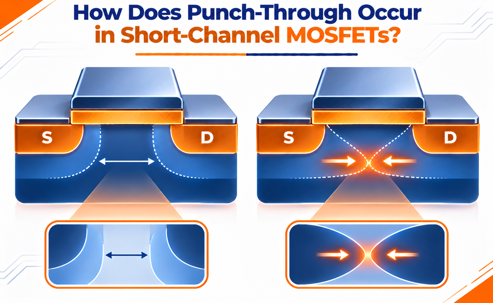
One important short-channel effect is punch-through. It occurs when the depletion regions surrounding the source and drain extend toward each other and become connected. When this happens, charge carriers can travel from the source to the drain through a region that is not effectively controlled by the gate.
As a result, the transistor may conduct even when the gate voltage is below the threshold voltage. This increases leakage current and weakens the ability of the MOSFET to switch completely OFF.
What Is Punch-Through in a MOSFET?
Punch-through is an unwanted condition in which the source and drain depletion regions expand sufficiently to connect beneath the channel.
In a conventional MOSFET, the gate controls the channel by regulating the potential barrier between the source and drain. When the gate voltage is low, this barrier prevents significant carrier flow.
However, in a short-channel MOSFET, the source and drain are positioned very close to each other. Their depletion regions can extend into the channel, particularly when the drain-to-source voltage increases.
When these depletion regions merge, the drain electric field can influence the source-side potential barrier. Carriers can then move through the depleted semiconductor beneath the surface, creating a current path that is not fully controlled by the gate.
This condition is known as punch-through.
Why Does Punch-Through Occur in Short-Channel MOSFETs?
Punch-through is mainly associated with the interaction between channel length, junction depletion width, substrate doping, and drain voltage.
Several factors contribute to its occurrence:
Reduced channel length: When the distance between the source and drain decreases, their depletion regions become more likely to interact.
High drain voltage: Increasing the drain-to-source voltage increases the reverse bias of the drain-to-body junction. This causes the drain depletion region to expand toward the source.
Low substrate doping: A lightly doped substrate generally produces wider depletion regions for a given junction voltage, increasing the possibility of depletion-region overlap.
Weak gate control: When the channel becomes very short, the drain electric field can influence the potential barrier near the source, reducing the gate’s ability to control carrier movement.
The combination of these conditions can create a continuous subsurface conduction path between the source and drain.
What Are the Effects of Punch-Through on MOSFET Performance?
Punch-through can negatively affect transistor operation in several ways.
Increased leakage current: Current flows between the source and drain even when the transistor is intended to remain OFF.
Poor switching behavior: The gate loses control over part of the carrier conduction path, reducing the effectiveness of transistor switching.
Higher static power consumption: Increased OFF-state current contributes to unwanted power dissipation.
Reduced noise margins: Uncontrolled current can affect logic voltage levels and circuit stability.
Device performance degradation: Excessive leakage can create additional thermal and power-management challenges in densely integrated circuits.
These effects become particularly important in low-power and high-density semiconductor applications.
How Can Punch-Through Be Prevented in Short-Channel MOSFETs?
Device engineers use several structural and process techniques to control depletion-region expansion and improve electrostatic behavior.
1. Halo or Pocket Implantation
Halo implantation introduces localized higher doping concentrations near the source and drain extensions.
This helps reduce depletion-region expansion and improves control of the potential barrier near the source.
It is widely used to manage short-channel effects in planar MOSFET technologies.
2. Increased Channel or Body Doping
Increasing the substrate or channel doping concentration reduces the depletion width for a given junction bias.
This makes it more difficult for the source and drain depletion regions to merge.
However, excessive doping can increase junction capacitance and mobility degradation, so the doping profile must be carefully optimized.
3. Shallow Source and Drain Junctions
Reducing the depth of source and drain junctions helps limit depletion-region expansion beneath the channel.
Shallow junction engineering can therefore reduce the possibility of subsurface punch-through.
4. Retrograde Well Engineering
A retrograde well uses a nonuniform doping profile, with higher doping deeper inside the semiconductor.
This helps restrict depletion-region expansion in the bulk while allowing a comparatively lower surface doping concentration.
5. Multi-Gate Transistor Structures
FinFETs and Gate-All-Around (GAA) transistors provide stronger electrostatic control by allowing the gate to control multiple sides of the channel.
This reduces the influence of the drain electric field on the source-side barrier and improves short-channel performance.
These structures do not automatically eliminate every leakage mechanism, but they offer better electrostatic control than conventional planar devices at comparable dimensions.
Why Is Punch-Through Control Important in Advanced Semiconductor Technology?
Modern processors, memory devices, mobile processors, and AI accelerators contain billions of transistors within a small chip area.
As transistor dimensions shrink, maintaining proper gate control becomes increasingly challenging.
Punch-through control is important because it helps:
- Reduce OFF-state leakage current.
- Improve transistor switching characteristics.
- Support low-power circuit operation.
- Maintain stable threshold-voltage behavior.
- Improve electrostatic control at smaller technology nodes.
- Enable reliable operation in high-density integrated circuits.
Advanced transistor architectures, optimized doping profiles, and carefully controlled junction geometries are therefore essential for managing punch-through and other short-channel effects.
Conclusion
Punch-through is an important short-channel effect that occurs when the depletion regions associated with the source and drain extend toward each other and create an uncontrolled conduction path.
It becomes more likely when the channel length is reduced, the drain voltage is increased, or the substrate doping is insufficient to restrict depletion-region expansion.
The resulting loss of gate control increases leakage current and affects transistor switching performance.
Techniques such as halo implantation, optimized body doping, shallow junction formation, retrograde wells, and multi-gate transistor architectures help reduce punch-through and improve the electrostatic performance of modern MOSFETs.
Understanding this mechanism is essential for semiconductor device engineers working on transistor scaling, process integration, and advanced CMOS technology.
Share your question in comments or talk to our mentor team for batch guidance.
Ask the Admin Team
Drop your basic question in comments: eligibility, prerequisites, tools, fee range, and placement support.
Our team reviews and responds regularly.