

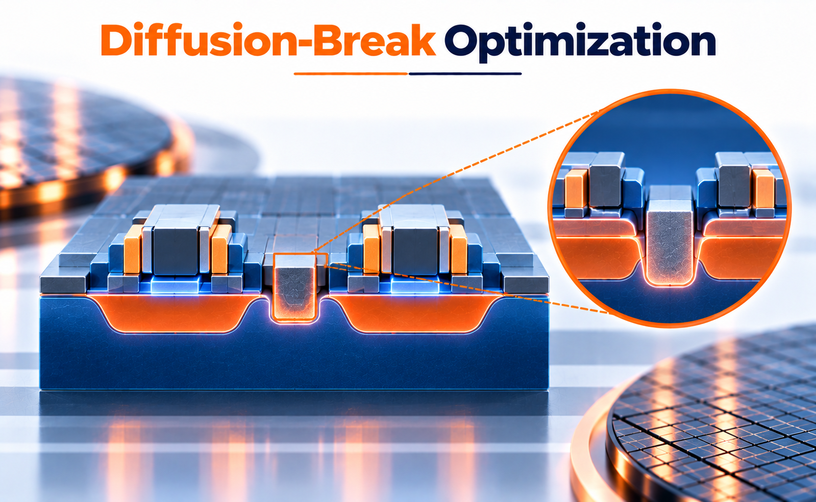
As semiconductor technology continues to scale, transistor dimensions and standard-cell layouts become increasingly compact. At advanced technology nodes, however, neighboring transistor regions cannot always be placed directly next to one another because unwanted electrical interaction, leakage, and process-related effects can occur.
Diffusion breaks are used to electrically isolate neighboring active regions. While they improve isolation, they also consume valuable layout area and can influence transistor performance through local layout effects and mechanical stress.
Diffusion-Break Optimization focuses on reducing these area and performance penalties while maintaining reliable device isolation. This has become an important design and process consideration for advanced FinFET and emerging gate-all-around (GAA) technologies.
What Is a Diffusion Break?
A diffusion break (DB) is a structure used to electrically isolate neighboring transistor active regions in a standard-cell layout.
In FinFET technologies, adjacent devices can share diffusion regions to improve area efficiency. However, where electrical isolation is required, a diffusion break is introduced between the active regions.
Two commonly discussed approaches are:
Single Diffusion Break (SDB)
An SDB uses a single isolation structure and can reduce the area consumed by the break compared with a double diffusion break.
Double Diffusion Break (DDB)
A DDB uses two dummy gates or equivalent isolation structures with an intervening isolation region. It provides robust separation but can introduce a larger area penalty.
Research has shown that SDB can be an effective area-scaling technique, while DDB can provide strong isolation at the cost of additional layout space.
Why Is Diffusion-Break Optimization Important?
At advanced nodes, every additional layout feature can have a significant impact on standard-cell density.
Area Reduction
Diffusion breaks consume horizontal layout space. Optimizing their structure can allow standard cells to become more compact.
Leakage Control
The diffusion-break structure helps prevent unwanted conduction between neighboring devices. Its geometry and neighboring structures can also influence leakage behavior.
Performance Control
Local layout effects associated with diffusion breaks can influence transistor delay and electrical characteristics. Research has shown that even the distance to a second-nearest diffusion break can affect device performance.
Variability Management
Changing the diffusion-break structure can alter the stress environment around neighboring transistors, potentially affecting device variability.
Therefore, optimization cannot focus on area alone. Area, leakage, timing, variability, stress, and manufacturability must be considered together.
Diffusion-Break Optimization in Advanced Nodes
As semiconductor architectures evolve, diffusion-break optimization is becoming increasingly relevant.
For FinFETs, SDB structures can provide area savings but may introduce more demanding process requirements. DDB structures provide a more conservative isolation approach but can consume additional cell area.
In emerging gate-all-around technologies, diffusion breaks can also become a device-performance engineering element rather than simply an isolation structure.
Recent 2026 research presented at the VLSI Symposium explored stressed single diffusion breaks as a potential performance and power-area-performance (PPA) enhancement mechanism for next-generation GAA logic. The study reported TCAD and calibrated circuit-model results indicating that engineered stress in SDB regions can influence nanosheet channel performance.
This illustrates an important shift: the diffusion break can be designed not only to isolate devices, but also to deliberately engineer the local mechanical environment.
The Future of Diffusion-Break Optimization
Future optimization is likely to involve a combination of device engineering, process integration, standard-cell architecture, and design automation.
Key development areas include:
- Smaller and more manufacturable SDB structures
- Improved diffusion-sharing techniques
- Stress-engineered diffusion breaks
- Better leakage-aware placement
- Reduced standard-cell area
- Improved process-window control
- Integration with GAA nanosheet architectures
- Diffusion-break-aware physical-design automation
- Improved variability and reliability management
Advanced physical-design flows will increasingly need to understand the relationship between cell placement, neighboring diffusion breaks, stress conditions, leakage, and timing. Research has already demonstrated that ignoring diffusion-break-dependent local effects can lead to inaccurate optimization decisions during placement and implementation.
Conclusion
Diffusion-Break Optimization is an important technology and design consideration for advanced CMOS scaling. Diffusion breaks provide essential electrical isolation between neighboring devices, but they also introduce area, process, leakage, stress, and performance trade-offs.
The evolution from DDB toward optimized SDB structures, together with diffusion sharing, reordering, self-aligned integration, and stress engineering, provides multiple approaches for reducing these penalties.
As semiconductor technology moves from FinFETs toward gate-all-around architectures, diffusion breaks are increasingly becoming part of the broader device-engineering strategy. Optimizing them will require simultaneous consideration of layout density, electrical isolation, stress, leakage, variability, manufacturability, and circuit performance.
Share your question in comments or talk to our mentor team for batch guidance.
Ask the Admin Team
Drop your basic question in comments: eligibility, prerequisites, tools, fee range, and placement support.
Our team reviews and responds regularly.