

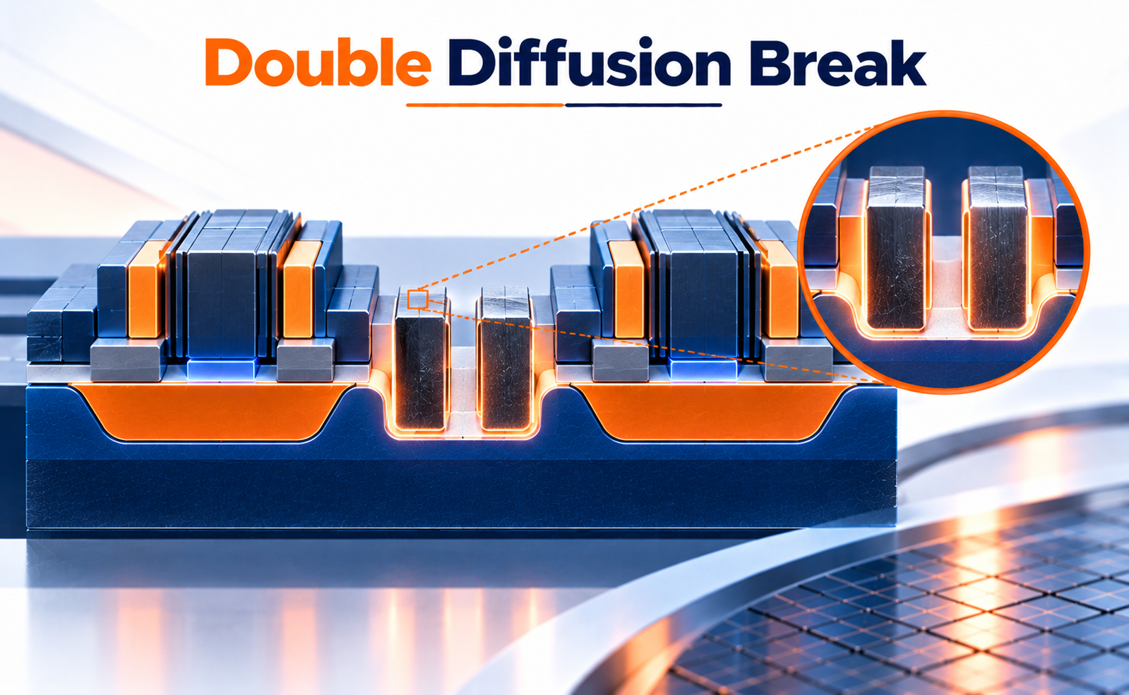
As semiconductor technology scales to smaller dimensions, transistor density and layout complexity continue to increase. In FinFET-based standard-cell design, neighboring transistors placed too closely can create unwanted leakage paths and electrical interactions. Double Diffusion Break (DDB) is one of the layout techniques used to provide stronger isolation between neighboring active regions.
DDB introduces additional gate structures between adjacent diffusion regions, helping control unwanted electrical interaction while maintaining the required device isolation. However, this isolation comes with an area penalty, making DDB an important topic in advanced standard-cell architecture and physical design optimization.
What Is a Double Diffusion Break?
A Double Diffusion Break is a structural isolation technique used in FinFET standard-cell layouts to separate neighboring diffusion regions.
In a conventional FinFET layout, active regions and transistor gates are arranged very densely. At the boundary between neighboring cells, unwanted leakage or electrical coupling can occur if the diffusion regions are not sufficiently isolated.
A DDB places two dummy gate structures between adjacent active transistor regions. These dummy structures help interrupt the continuous diffusion path and provide greater isolation between neighboring devices.
Compared with a Single Diffusion Break (SDB), which uses one break structure, DDB provides a wider isolation region. This makes it useful where the process technology or design rules require stronger separation.
Why Is DDB Important in FinFET Technology?
As transistor dimensions shrink, physical spacing becomes increasingly important. Closely positioned FinFET devices can experience unwanted electrical interaction, including leakage through regions beneath dummy gates.
DDB addresses this problem by increasing the separation between neighboring active regions.
Its key purposes include:
- Reducing unwanted leakage paths
- Improving electrical isolation between neighboring cells
- Controlling interactions between adjacent FinFET structures
- Supporting reliable standard-cell operation
- Meeting process-specific layout requirements
This makes DDB particularly relevant to standard-cell libraries where thousands or millions of cells may be placed next to one another.
However, better isolation does not come for free. The additional dummy-gate structures consume layout space and can reduce overall cell density.
DDB and the Standard-Cell Area Penalty
One of the biggest challenges associated with DDB is area overhead.
A DDB at the edge of a standard cell can require additional layout space for the two dummy gates. When these structures are repeated across a large block, the accumulated area penalty can become significant.
The impact becomes especially important in high-density digital designs where standard-cell utilization directly affects:
- Logic density
- Die area
- Routing resources
- Placement flexibility
- Overall PPA optimization
Research published in IEICE Transactions on Fundamentals describes how DDB structures in early FinFET processes can require additional unit-cell space at cell boundaries. The researchers proposed alternative cell structures and diffusion reordering to reduce this penalty.
This illustrates an important principle in advanced physical design: isolation must be balanced against density.
DDB Challenges in Advanced Semiconductor Nodes
Although DDB provides effective isolation, its implementation introduces several design challenges.
Area Overhead
The additional dummy structures increase cell dimensions and can reduce transistor density.
Routing Complexity
Extra structures at cell boundaries can influence available routing resources and complicate placement.
Library Design
Standard-cell libraries must maintain consistent cell heights, boundary conditions, electrical characteristics, and manufacturability requirements.
Leakage and Reliability Trade-offs
Removing or reducing diffusion breaks may improve density, but isolation requirements cannot simply be ignored. Any optimization must satisfy the technology’s electrical and manufacturing constraints.
Process Dependence
The preferred diffusion-break architecture depends strongly on the semiconductor process and its design rules. Therefore, a layout strategy that works for one FinFET generation may not directly apply to another.
These trade-offs make DDB optimization a combined device, process, standard-cell, and physical-design problem rather than simply a layout-spacing problem.
The Future of Diffusion-Break Optimization
As semiconductor technology continues toward increasingly dense FinFET and gate-all-around transistor architectures, diffusion-break structures will remain an important consideration in device isolation and standard-cell design.
Future optimization is likely to focus on reducing the area cost of isolation while preserving electrical performance, leakage control, reliability, and manufacturability.
Research directions include:
- More efficient standard-cell boundary architectures
- Intelligent diffusion sharing
- Automated transistor and diffusion reordering
- Process-aware cell-library optimization
- Advanced isolation structures
- Co-optimization of device and physical layout
- Design automation techniques for minimizing diffusion-break overhead
The broader objective is to achieve a better balance between isolation, density, leakage, performance, and manufacturability.
Conclusion
Double Diffusion Break is an important isolation technique in FinFET-based standard-cell design. By introducing two dummy gate structures between neighboring active regions, DDB can help control unwanted leakage and electrical interaction.
At the same time, the additional structures create an area penalty that becomes increasingly significant in highly scaled designs. As a result, advanced semiconductor design increasingly focuses on optimizing cell architecture, diffusion sharing, and transistor ordering to reduce the cost of DDB.
Ultimately, DDB optimization represents a broader challenge in semiconductor scaling: achieving strong device isolation without sacrificing the density and efficiency required by modern VLSI designs.
Share your question in comments or talk to our mentor team for batch guidance.
Ask the Admin Team
Drop your basic question in comments: eligibility, prerequisites, tools, fee range, and placement support.
Our team reviews and responds regularly.