

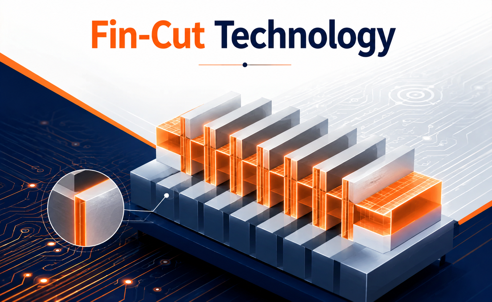
As semiconductor technology continues to evolve, traditional transistor architectures are approaching their physical and performance limits. The industry is therefore moving toward advanced transistor structures that can deliver greater performance, improved energy efficiency, and higher transistor density.
Fin-Cut Technology is an important advancement in this evolution. By precisely defining and separating transistor fins during fabrication, Fin-Cut processes enable better control over transistor dimensions and help semiconductor manufacturers build increasingly sophisticated chip architectures.
From high-performance processors to AI accelerators and advanced SoCs, Fin-Cut technology plays a significant role in enabling the next generation of semiconductor devices.
What Is Fin-Cut Technology?
Fin-Cut Technology is a semiconductor manufacturing technique used primarily with FinFET-based transistor architectures.
In a FinFET, the transistor channel is formed as a thin, vertical fin. The gate surrounds multiple sides of this fin, providing improved control over the flow of current compared with traditional planar transistors.
The Fin-Cut process introduces an additional patterning and etching step to precisely remove portions of these fins. This allows manufacturers to define where individual transistor structures begin and end.
Why Is Fin-Cut Technology Important?
At advanced semiconductor nodes, even extremely small variations in transistor geometry can affect chip performance, power consumption, and manufacturing yield.
Fin-Cut technology helps address these challenges by providing greater control over transistor isolation and geometry.
Fin-Cut Technology in Advanced Semiconductor Manufacturing
The importance of Fin-Cut technology becomes particularly evident at advanced process nodes, where semiconductor manufacturers must manage extremely small dimensions and increasingly complex layouts.
Modern chips can contain billions of transistors, and each transistor must operate reliably within strict manufacturing tolerances.
The Future of Fin-Cut Technology
The semiconductor industry is moving beyond conventional FinFET architectures toward technologies such as Gate-All-Around (GAA) transistors and eventually more advanced transistor structures.
While transistor architectures are changing, the underlying requirement remains the same: precise nanoscale manufacturing control.
Fin-Cut technology represents an important stage in this progression. It demonstrates how seemingly small fabrication innovations can have a major impact on transistor scaling, chip density, power efficiency, and performance.
Conclusion
Fin-Cut Technology is more than simply an additional fabrication step. It is part of the sophisticated manufacturing ecosystem that allows semiconductor companies to continue pushing the boundaries of transistor scaling.
As demand grows for AI processors, high-performance computing, automotive electronics, edge devices, and energy-efficient chips, advanced semiconductor manufacturing techniques such as Fin-Cut will remain essential to the industry’s progress.
Share your question in comments or talk to our mentor team for batch guidance.
Ask the Admin Team
Drop your basic question in comments: eligibility, prerequisites, tools, fee range, and placement support.
Our team reviews and responds regularly.