

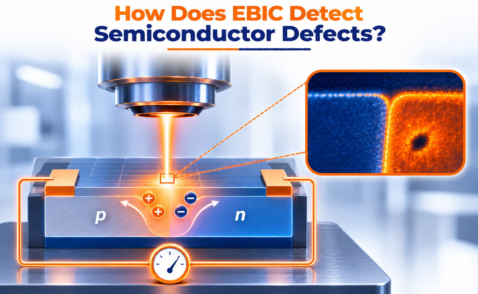
Electron Beam Induced Current (EBIC) is a semiconductor characterization technique used to investigate defects, junction properties, and charge-collection behavior in semiconductor devices. It is particularly useful for identifying defects that affect the movement and collection of charge carriers.
During semiconductor manufacturing, defects such as dislocations, recombination centers, junction irregularities, and electrically inactive regions can influence device performance. Some of these defects are difficult to identify using conventional imaging techniques because they may not produce visible structural changes.
EBIC helps overcome this limitation by combining a focused electron beam with electrical current measurements. When the electron beam interacts with a semiconductor, it generates electron-hole pairs. The way these carriers move and are collected provides valuable information about the electrical quality of the material.
What Is Electron Beam Induced Current (EBIC)?
Electron Beam Induced Current (EBIC) is an electron microscopy-based technique that measures the current generated when a focused electron beam interacts with a semiconductor.
When high-energy electrons from a scanning electron microscope (SEM) strike a semiconductor surface, they transfer energy to the material and generate electron-hole pairs.
These charge carriers move through the semiconductor. If an electric field is present, such as at a p-n junction or a Schottky barrier, the carriers can be separated and collected by electrical contacts.
The resulting current is known as the electron beam induced current.
EBIC measurements are commonly used to study:
- p-n junction locations and electrical behavior.
- Carrier collection efficiency.
- Recombination-active defects.
- Dislocations and extended defects.
- Electrically inactive regions.
- Junction leakage and local electrical nonuniformities.
Unlike conventional electron microscopy, which primarily provides structural information, EBIC reveals how different regions of a semiconductor contribute to electrical charge collection.
How Does EBIC Identify Semiconductor Defects?
The key principle behind EBIC defect detection is that defects can change the lifetime, diffusion, recombination, and collection of charge carriers.
In a relatively defect-free semiconductor region, generated carriers can travel toward the junction and contribute to the measured current.
However, defects may introduce energy states within the semiconductor bandgap. These states can act as recombination centers, reducing the number of carriers available for collection.
As a result, defective regions may produce a lower EBIC signal than surrounding regions.
Some important defects that can be investigated using EBIC include:
Dislocations: Dislocations can introduce electrically active states that increase carrier recombination. They may appear as localized regions of reduced EBIC signal.
Recombination centers: Impurities, crystal imperfections, and other defects can create energy levels within the bandgap, reducing minority-carrier lifetime and collection efficiency.
Junction defects: Irregularities in p-n junctions can influence the local electric field and carrier collection behavior.
Crystalline defects: Certain structural defects can affect carrier transport and produce variations in the EBIC signal.
Electrically inactive regions: Areas with poor carrier collection may appear darker or exhibit reduced current intensity in an EBIC image.
It is important to understand that a dark EBIC region does not automatically indicate a specific defect. Signal variations must be interpreted alongside material structure, sample preparation, and other characterization results.
What Information Can EBIC Images Reveal?
An EBIC image provides spatial information about how efficiently different regions of a semiconductor collect generated charge carriers.
The contrast in an EBIC image is primarily related to the local induced current.
Some important observations include:
- Bright regions: Often indicate stronger carrier collection under the selected imaging conditions.
- Dark regions: May indicate reduced carrier collection, enhanced recombination, or electrically inactive areas.
- Localized contrast variations: Can reveal isolated defects or nonuniform electrical behavior.
- Junction contrast: Helps identify the location and electrical response of semiconductor junctions.
- Extended dark features: May indicate dislocations, defect clusters, or other recombination-active structures.
For example, when an electron beam scans across a semiconductor containing a p-n junction, the depletion region can produce a strong EBIC response because its electric field helps separate and collect electron-hole pairs.
If a recombination-active defect exists near the junction, the local current may decrease, creating a contrast variation in the resulting image.
The interpretation depends on the beam conditions, device geometry, junction orientation, and carrier transport properties.
What Are the Applications of EBIC in Semiconductor Manufacturing?
EBIC is used in semiconductor research, process development, and failure analysis to investigate electrical defects that may affect device performance.
Solar cell characterization: EBIC helps identify recombination-active regions, grain boundaries, and defects that reduce carrier collection efficiency in photovoltaic materials.
Power semiconductor analysis: It can be used to investigate defects and carrier collection behavior in devices such as silicon and silicon carbide structures.
Junction characterization: EBIC helps identify junction locations and evaluate local electrical behavior in semiconductor devices.
Failure analysis: Engineers can investigate localized regions with reduced carrier collection to identify possible electrically active defects.
Compound semiconductor research: EBIC is useful for examining defects in materials such as GaAs, GaN, and other compound semiconductors.
Process development: Researchers can compare samples produced under different manufacturing conditions to understand how processing influences electrical quality.
What Are the Advantages and Limitations of EBIC?
EBIC provides valuable electrical information that complements conventional electron microscopy techniques.
Advantages
- Provides spatially resolved information about carrier collection.
- Helps identify recombination-active defects.
- Supports p-n junction characterization.
- Can investigate defects that are not easily identified through conventional structural imaging.
- Can be integrated with SEM-based characterization.
- Useful for semiconductor research and failure analysis.
Limitations
- Requires suitable electrical contacts and measurement configurations.
- Sample preparation can influence the measured signal.
- Defect identification may require additional characterization techniques.
- Signal interpretation depends on beam energy, carrier diffusion, and device geometry.
- Some defects may not produce sufficient EBIC contrast for reliable detection.
- EBIC images alone generally cannot determine the exact chemical or structural identity of a defect.
For this reason, EBIC is often combined with techniques such as SEM imaging, transmission electron microscopy (TEM), cathodoluminescence (CL), and other electrical measurements.
Conclusion
Electron Beam Induced Current is a valuable characterization technique for understanding electrical defects and charge-carrier behavior in semiconductor materials.
By generating electron-hole pairs with a focused electron beam and measuring the resulting current, EBIC reveals variations in carrier collection across a semiconductor structure.
This makes it useful for investigating dislocations, recombination centers, junction irregularities, and electrically inactive regions.
Share your question in comments or talk to our mentor team for batch guidance.
Ask the Admin Team
Drop your basic question in comments: eligibility, prerequisites, tools, fee range, and placement support.
Our team reviews and responds regularly.