

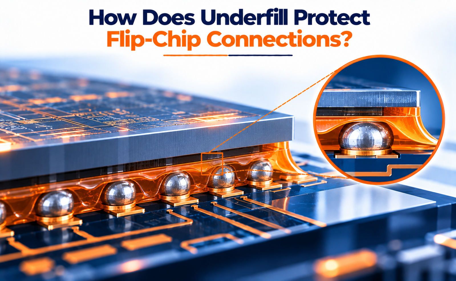
Flip-chip packaging enables semiconductor dies to connect directly to substrates through an array of microscopic solder bumps or other interconnect structures. This architecture provides short electrical paths, high I/O density, and excellent electrical performance, making it widely used in advanced semiconductor packages.
However, the tiny solder connections between the die and substrate are exposed to significant mechanical and thermal stresses during manufacturing and operation. Underfill is used to address these reliability challenges.
Underfill is a polymeric material introduced into the narrow gap between the semiconductor die and substrate. Once cured, it forms a mechanically supportive layer around the interconnects, helping distribute stresses and protect the flip-chip assembly.
What Is Underfill in Flip-Chip Packaging?
In a flip-chip package, the semiconductor die is mounted face-down onto a substrate. An array of solder bumps provides both the mechanical and electrical connection between the die and substrate.
After the die is attached, a gap remains between the two surfaces.
Underfill is a liquid or flowable material that is introduced into this gap and subsequently cured.
A simplified structure is:
Semiconductor Die
↓
Underfill Material
↓
Solder Bumps / Interconnects
↓
Package Substrate
The underfill surrounds the solder bumps and creates a continuous mechanical structure between the die and substrate.
Depending on the package and manufacturing process, underfill may be applied using different approaches, including:
- Capillary underfill
- Molded underfill
- No-flow underfill
- Pre-applied or wafer-level underfill materials
The primary purpose is to improve the mechanical and thermal reliability of the flip-chip interconnections.
Why Do Flip-Chip Connections Need Underfill?
Flip-chip solder joints are extremely small, and the die and substrate are generally made from materials with different coefficients of thermal expansion (CTE).
When the package experiences a temperature change, these materials expand and contract at different rates.
For example:
Silicon die → low CTE
Organic substrate → higher CTE
During temperature cycling, this mismatch creates mechanical strain in the solder bumps.
Without adequate stress management, repeated thermal cycling can contribute to:
- Solder fatigue
- Crack formation
- Interconnect failure
- Delamination
- Electrical opens
- Reduced package lifetime
Underfill helps address this problem by mechanically coupling the die and substrate.
Instead of allowing individual solder bumps to absorb most of the thermomechanical deformation, the cured underfill distributes a portion of the stress across the larger package structure.
This makes underfill particularly important for packages containing fine-pitch and high-density flip-chip interconnections.
Underfill Materials and the Manufacturing Process
Underfill materials are typically polymer-based systems formulated to provide the required combination of flow, adhesion, mechanical strength, thermal properties, and reliability.
Common formulations use epoxy-based materials containing carefully engineered fillers and additives.
A simplified capillary-underfill process is:
Step 1: Flip-Chip Attachment
The semiconductor die is aligned and attached to the substrate through the solder-bump array.
Step 2: Underfill Dispensing
Liquid underfill material is dispensed along one or more edges of the die.
Step 3: Capillary Flow
The material flows through the narrow gap between the die and substrate, surrounding the solder bumps.
Step 4: Void Control
The process is controlled to minimize trapped air and incomplete filling.
Step 5: Curing
The filled package is heated according to the material’s cure profile, converting the liquid underfill into a solid mechanical structure.
The manufacturing process must carefully control viscosity, dispensing conditions, flow behavior, temperature, and cure conditions.
Incomplete filling or trapped voids can create localized reliability problems.
Key Challenges in Underfill Technology
Although underfill significantly improves flip-chip reliability, introducing it into advanced packages creates its own engineering challenges.
Void Formation
Air pockets or unfilled regions can develop during underfill flow. Voids may reduce mechanical support and create localized stress concentrations.
Warpage
Underfill materials and package components can have different CTEs and mechanical properties. During curing and temperature cycling, these differences can contribute to package warpage.
Delamination
Poor adhesion between the underfill and die, substrate, or solder structures can result in interfacial delamination.
Moisture Absorption
Polymeric materials can absorb moisture, which may affect mechanical and electrical reliability during subsequent thermal processing or operation.
Fine-Pitch Filling
As the distance between the die and substrate becomes smaller and bump density increases, completely filling the gap becomes increasingly challenging.
Material Selection
The underfill must provide an appropriate balance between:
- Low CTE
- Suitable modulus
- Strong adhesion
- Controlled viscosity
- Good flow characteristics
- Thermal stability
- Moisture resistance
- Reliable curing
Therefore, underfill development involves both materials engineering and package-process optimization.
The Future of Underfill for Advanced Packaging
As semiconductor packages move toward higher I/O density, smaller bump pitches, chiplets, 2.5D integration, and 3D architectures, underfill technology will continue to evolve.
Future developments are likely to focus on:
- Faster-flowing underfill materials
- Low-temperature curing
- Reduced warpage
- Improved adhesion
- Lower-stress formulations
- Better void control
- Fine-pitch compatibility
- Advanced filler engineering
- Improved thermal performance
- Materials optimized for chiplet and 3D packaging
Advanced packages also require underfill materials to work alongside increasingly complex structures such as high-density substrates, redistribution layers, interposers, microbumps, and hybrid-bonding interfaces.
The objective is no longer simply to fill the space beneath a flip-chip die. The material must be engineered as an integral part of the package’s mechanical, thermal, and reliability architecture.
Conclusion
Underfill plays a critical role in protecting flip-chip connections from thermomechanical stress and improving package reliability.
By filling the space between the semiconductor die and substrate, underfill mechanically couples the two structures and helps distribute stresses caused by differences in thermal expansion.
This reduces stress concentration around individual solder bumps and can significantly improve resistance to thermal cycling and mechanical loading.
As flip-chip packages continue to evolve toward finer pitches, higher I/O density, chiplets, 2.5D integration, and 3D packaging, advanced underfill materials will remain an important technology for achieving reliable semiconductor interconnections.
Share your question in comments or talk to our mentor team for batch guidance.
Ask the Admin Team
Drop your basic question in comments: eligibility, prerequisites, tools, fee range, and placement support.
Our team reviews and responds regularly.