

What Is Analog Layout Design?
Analog Layout Design is the process of converting an analog circuit schematic into a physical layout that can be fabricated on a semiconductor wafer. It involves placing transistors and other electronic components and connecting them through metal interconnects while following the manufacturing rules of a semiconductor process.
Unlike digital circuits, analog circuits are highly sensitive to physical variations, noise, parasitic capacitance, resistance and device mismatches. Therefore, analog layout engineers must carefully consider the physical arrangement of components to ensure the circuit performs as intended.
Analog layout is an essential part of VLSI design because it directly influences the performance, reliability and functionality of analog integrated circuits.
From Circuit Schematic to Physical Layout
Analog IC design begins with a circuit schematic that defines the electrical connections and behaviour of the circuit. The layout engineer converts this schematic into a physical representation using a layout design tool.
The process typically includes:
- Identifying circuit components such as MOSFETs, resistors and capacitors.
- Determining device dimensions and finger configurations.
- Placing components according to circuit requirements.
- Routing connections using different metal layers.
- Following foundry-specific design rules.
The resulting layout represents the physical structure of the circuit that will be manufactured on silicon. After layout completion, it undergoes physical verification and parasitic extraction before final sign-off.
Understanding Analog Layout Components and Layers
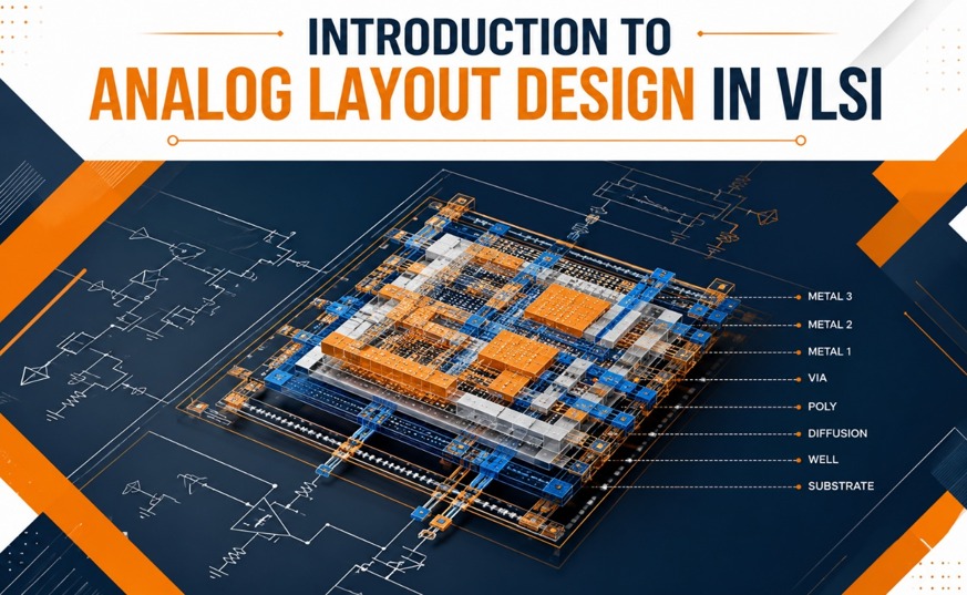
Analog layout is built using different layers of a semiconductor process. Each layer serves a specific purpose in creating transistors, interconnections and passive components.
Common layout elements include:
- Active/Diffusion Layer: Defines semiconductor regions used to form transistor source and drain regions.
- Poly Layer: Used to form transistor gates in traditional CMOS processes.
- Metal Layers: Provide electrical connections between devices and circuit components.
- Contact and Via Layers: Connect device regions and different metal layers.
- Well Layers: Create regions for NMOS and PMOS devices and support isolation and device operation.
Layout engineers use these layers to build circuit structures while following the Process Design Kit (PDK) and technology-specific design rules.
Understanding Analog Layout Components and Layers
Analog layout is built using different layers of a semiconductor process. Each layer serves a specific purpose in creating transistors, interconnections and passive components.
Common layout elements include:
- Active/Diffusion Layer: Defines semiconductor regions used to form transistor source and drain regions.
- Poly Layer: Used to form transistor gates in traditional CMOS processes.
- Metal Layers: Provide electrical connections between devices and circuit components.
- Contact and Via Layers: Connect device regions and different metal layers.
- Well Layers: Create regions for NMOS and PMOS devices and support isolation and device operation.
Layout engineers use these layers to build circuit structures while following the Process Design Kit (PDK) and technology-specific design rules.
Key Principles of Analog Layout Design
Analog layout requires careful physical implementation because layout geometry can affect electrical performance.
Important design principles include:
- Matching: Placing similar devices carefully to reduce mismatch in their electrical characteristics.
- Symmetry: Using symmetrical placement and routing to improve circuit balance.
- Common-Centroid Layout: Arranging matched devices to reduce the impact of process gradients.
- Guard Rings: Using surrounding structures to help isolate sensitive circuits from substrate noise.
- Parasitic Reduction: Minimising unwanted resistance and capacitance from devices and interconnects.
These techniques are commonly used in precision analog circuits, differential pairs, current mirrors, amplifiers and other sensitive circuit blocks.
Analog Layout Design Flow
Analog layout follows a structured workflow to transform a circuit schematic into a physical design ready for fabrication.
The major steps involved are:
- Schematic Review: Understand the circuit connections, device sizes and performance requirements.
- Floorplanning: Define the placement arrangement of circuit blocks and important devices.
- Placement: Position transistors and passive components according to matching, symmetry and circuit requirements.
- Routing: Connect devices using metal layers while considering noise, parasitics and routing constraints.
- DRC (Design Rule Check): Verify whether the layout satisfies manufacturing design rules.
- LVS (Layout Versus Schematic): Check whether the physical layout matches the intended schematic connectivity.
- Parasitic Extraction and Post-Layout Simulation: Extract parasitic effects and evaluate how they impact circuit performance.
Each stage helps improve layout quality and ensures the design is ready for physical verification and sign-off.
Applications and Importance of Analog Layout in the Semiconductor Industry
Analog layout design is used across various semiconductor applications where circuits interact with real-world signals, power supplies and electronic systems.
Major applications include:
- Power Management ICs (PMICs): Voltage regulators, power converters and battery management circuits.
- Communication ICs: RF front ends, signal amplifiers and high-frequency circuits.
- Mixed-Signal ICs: Chips combining analog and digital circuits, such as ADCs and DACs.
- Automotive Electronics: Sensor interfaces, power control, signal conditioning and vehicle electronic systems.
- Consumer Electronics: Analog circuits used in smartphones, audio devices, wearable electronics and other products.
Analog layout engineers play an important role in achieving accurate circuit performance, reliable operation and manufacturable designs across these applications.
Conclusion
Analog Layout Design is a fundamental part of the VLSI and semiconductor industry, bridging circuit schematics and physical silicon implementation. It requires a strong understanding of CMOS devices, layout layers, placement, routing, matching techniques, parasitic effects and physical verification.
As semiconductor technology continues to advance, analog layout remains important in developing high-performance, low-power and reliable integrated circuits for modern electronic applications.
Understanding analog layout fundamentals is an important first step for anyone interested in building a career in Analog Layout Design and semiconductor engineering.
Share your question in comments or talk to our mentor team for batch guidance.
Need Fee, Duration, or Demo Class Details?
Talk to our admin team for the latest batch plan and career guidance.
Contact Admin TeamAsk the Admin Team
Drop your basic question in comments: eligibility, prerequisites, tools, fee range, and placement support.
Our team reviews and responds regularly.