

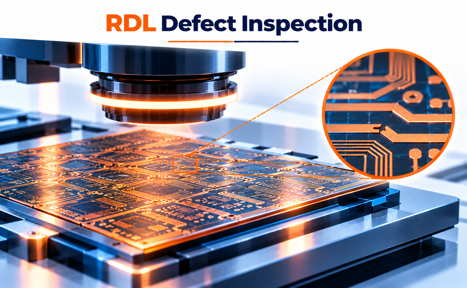
As semiconductor packaging continues to evolve toward fan-out wafer-level packaging, fan-out panel-level packaging, chiplets, and heterogeneous integration, Redistribution Layers (RDLs) have become increasingly important. RDLs provide electrical connections between chip I/O locations and external interconnect structures, enabling more flexible and higher-density package architectures.
As RDL dimensions shrink, however, even small defects in metal traces, dielectric layers, vias, or interfaces can affect electrical connectivity and package yield. RDL defect inspection therefore plays a critical role in identifying manufacturing abnormalities before they propagate into later packaging stages.
Modern inspection approaches combine high-resolution imaging, automated optical inspection, metrology, defect classification, and data analysis to detect and characterize RDL defects across wafers, panels, and packaged devices.
What Is RDL Defect Inspection?
RDL defect inspection is the process of examining redistribution-layer structures to identify defects that could affect electrical performance, reliability, or manufacturing yield.
An RDL typically consists of patterned metal traces embedded within or surrounded by dielectric material. Depending on the packaging technology, multiple RDL layers may be stacked to provide high-density routing.
Inspection can focus on:
- Metal traces
- Vias and via connections
- Line width and spacing
- Dielectric openings
- Metal continuity
- Surface contamination
- Pattern deformation
- RDL-to-pad connections
- Layer-to-layer alignment
The objective is not simply to detect a visible anomaly. Inspection systems must determine whether the observed variation represents a true manufacturing defect or an acceptable process variation.
This distinction becomes increasingly important as RDL line/space dimensions move toward finer geometries.
Common RDL Defects
RDL manufacturing involves multiple processes, including dielectric deposition, lithography, etching, seed-layer formation, copper plating, planarization, and cleaning. Defects can therefore originate at several stages.
Open Circuits
A discontinuity in an RDL trace can interrupt the electrical path between two connection points.
Possible causes include incomplete metal deposition, plating problems, lithographic defects, or pattern damage.
Shorts
Unwanted electrical connections can occur when excess metal remains between neighboring traces.
Shorts can result from insufficient pattern separation, plating abnormalities, particles, or lithography-related issues.
Line-Width Variations
Variations in RDL trace dimensions can affect resistance and signal integrity.
Excessive narrowing may increase electrical resistance, while excessive widening can reduce spacing to adjacent structures.
Via Defects
RDL vias provide vertical electrical connections between different layers. Voids, incomplete filling, misalignment, or poor interfaces can compromise these connections.
Metal Voids
Voids within copper features can reduce effective cross-sectional area and create potential reliability problems.
Particle and Contamination Defects
Foreign particles can interfere with lithography, plating, bonding, or dielectric formation, potentially creating localized RDL defects.
Why Is RDL Inspection Important?
RDLs are increasingly used to support high-density package architectures, making their manufacturing quality directly connected to package yield and reliability.
A small defect can have consequences beyond the immediate RDL layer.
For example, an open trace can disconnect an I/O path, while a short can create an unwanted electrical connection. Dimensional variations can also influence resistance, signal behavior, and the reliability of neighboring structures.
RDL inspection therefore helps manufacturers:
- Improve package yield
- Detect process excursions
- Reduce defect escapes
- Monitor critical dimensions
- Identify systematic defects
- Improve process control
- Support root-cause analysis
- Protect downstream packaging operations
Defect inspection also becomes valuable when analyzing spatial defect patterns. If defects repeatedly occur in specific wafer or panel regions, engineers can investigate relationships with lithography fields, plating uniformity, equipment conditions, or process non-uniformity.
Challenges in RDL Defect Inspection
As RDL technology scales, inspection becomes more difficult.
Fine Line/Space
Smaller RDL geometries require higher imaging resolution and greater defect sensitivity.
Complex Multilayer Structures
Multiple RDL layers increase the number of interfaces and alignment relationships that must be controlled.
Surface Topography
Copper and dielectric structures can produce significant surface-height variations, making high-quality imaging and measurement more challenging.
High Inspection Throughput
Large wafers and panels contain enormous inspection areas. Systems must detect very small defects without making inspection prohibitively slow.
False Positives
Manufacturing processes naturally introduce some variation. Inspection systems must distinguish real defects from acceptable process variation.
Defect Classification
Simply detecting a defect is not enough. Engineers need to understand whether it is related to lithography, plating, dielectric processing, contamination, mechanical damage, or another source.
Machine-learning-based classification and automated defect review are increasingly being investigated to address this challenge.
Conclusion
RDL defect inspection is a critical quality-control step in advanced semiconductor packaging.
By detecting opens, shorts, dimensional variations, via defects, voids, contamination, and alignment problems, inspection systems help manufacturers maintain the electrical and physical integrity of redistribution layers.
As fan-out packaging, chiplets, heterogeneous integration, and high-density RDL architectures continue to develop, inspection requirements will become increasingly demanding.
The combination of high-resolution imaging, precision metrology, automated classification, defect mapping, and AI-assisted analysis can help semiconductor manufacturers move toward higher-yield and more reliable advanced packaging processes.
Share your question in comments or talk to our mentor team for batch guidance.
Ask the Admin Team
Drop your basic question in comments: eligibility, prerequisites, tools, fee range, and placement support.
Our team reviews and responds regularly.