

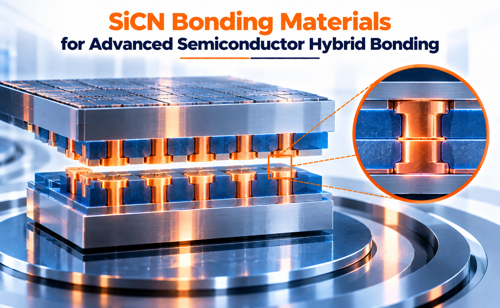
As semiconductor systems move toward finer interconnect pitches and increasingly complex 3D architectures, conventional packaging approaches are facing significant scaling challenges. Hybrid bonding has emerged as an important technology for vertically integrating memory, logic, chiplets, and other heterogeneous devices without relying on conventional solder-based interconnects.
Within hybrid bonding, the dielectric material surrounding the copper interconnects plays a critical role. Silicon Carbon Nitride (SiCN) has attracted significant attention because it can provide strong dielectric-to-dielectric bonding, copper diffusion protection, mechanical robustness, and compatibility with fine-pitch integration. Research and demonstrations have shown Cu/SiCN hybrid bonding at increasingly small interconnect pitches, including 400 nm and more recently 200 nm in wafer-to-wafer research.
What Is SiCN in Hybrid Bonding?
Silicon Carbon Nitride (SiCN) is a dielectric material composed primarily of silicon, carbon, and nitrogen. In advanced hybrid bonding, it can serve as the dielectric surface surrounding embedded copper pads.
Unlike conventional bonding approaches where solder or other intermediate materials connect two devices, hybrid bonding directly joins:
- Cu to Cu for the electrical connection
- SiCN to SiCN for the surrounding dielectric interface
This creates a highly integrated interface between two semiconductor surfaces.
The dielectric is not simply an insulating layer. It also helps establish the surface topography, provides mechanical support, electrically isolates neighboring interconnects, and contributes to the overall reliability of the bonded structure.
SiCN is particularly attractive for fine-pitch applications because its bonding interface can provide higher bonding strength than SiO₂ in reported studies, while also functioning as a copper diffusion barrier and passivation layer.
Why Is SiCN Important for Advanced Hybrid Bonding?
As interconnect pitch decreases, the amount of space available around each copper connection becomes extremely small. This places increasingly strict requirements on the dielectric material.
SiCN offers several characteristics that make it attractive for advanced hybrid bonding:
High Bond Strength
The SiCN-to-SiCN interface can achieve strong bonding after relatively low-temperature annealing. This is important when stacking devices that contain temperature-sensitive structures.
Copper Diffusion Barrier
SiCN can act as a barrier against copper diffusion, helping protect surrounding dielectric and device structures.
Mechanical Stability
The dielectric interface must withstand mechanical stresses during bonding, annealing, handling, and subsequent processing.
Fine-Pitch Compatibility
The combination of SiCN bonding and precise copper-pad control has enabled research demonstrations at very small interconnect pitches. Imec has reported Cu/SiCN wafer-to-wafer bonding at 400 nm pitch, while a later demonstration reached 200 nm interconnect pitch.
These properties make SiCN particularly relevant to next-generation 3D integration.
Material and Surface Engineering of SiCN
The performance of SiCN bonding depends not only on the material itself but also on its composition, deposition conditions, surface chemistry, roughness, and activation process.
The SiCN film must provide an appropriate balance between mechanical properties, chemical reactivity, surface quality, and thermal stability.
Surface activation is especially important. Recent research indicates that plasma treatment can modify the SiCN surface and create reactive sites that promote interfacial bonding. One 2025 IEEE study reported that plasma-treated SiCN could achieve strong, void-free bonding at 250°C and suggested a bonding mechanism involving transformation of the surface toward a thin silica-like layer rather than relying solely on hydroxyl density.
Deposition technology is another area of optimization. PECVD is commonly investigated for SiCN film formation, while research has also explored PVD SiCN as an alternative approach. Reported work found that PVD process parameters can influence film density, refractive index, carbon and nitrogen content, and therefore the resulting film properties.
This means that SiCN material engineering and bonding-process engineering must be considered together.
Future of SiCN Bonding Materials
SiCN is becoming an important material platform for advanced hybrid bonding because it combines dielectric functionality with properties that support fine-pitch integration.
Future development is likely to focus on:
- Lower-temperature bonding
- Improved plasma surface activation
- Ultra-flat CMP processes
- Better control of SiCN composition
- Reduced surface contamination
- Improved copper diffusion protection
- Higher bonding strength
- Better wafer-level uniformity
- Sub-200 nm interconnect scaling
- Improved reliability for 3D memory and logic integration
Recent demonstrations already show the direction of this technology. Imec has reported 200 nm-pitch wafer-to-wafer hybrid bonding using SiCN as the dielectric material, while research is continuing toward even smaller pitches.
At the same time, research into low-temperature SiCN activation and bonding is exploring ways to reduce thermal budgets while maintaining strong interfaces.
Conclusion
SiCN is more than an insulating material in advanced hybrid bonding—it is a critical part of the bonding interface itself.
Its combination of bonding strength, copper diffusion resistance, mechanical stability, surface-process compatibility, and fine-pitch potential makes it highly relevant to next-generation 3D semiconductor integration.
As hybrid bonding moves toward increasingly dense interconnects, success will depend on the co-optimization of SiCN material composition, deposition, CMP, surface activation, copper geometry, alignment, bonding, and annealing.
The continued development of SiCN bonding materials could therefore play an important role in enabling future memory-on-logic, logic-on-logic, chiplet, and heterogeneous 3D semiconductor architectures.
Share your question in comments or talk to our mentor team for batch guidance.
Ask the Admin Team
Drop your basic question in comments: eligibility, prerequisites, tools, fee range, and placement support.
Our team reviews and responds regularly.