

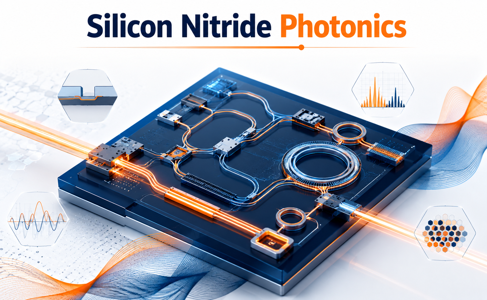
Silicon Nitride (SiN) photonics is emerging as a powerful platform for building high-performance optical circuits on semiconductor chips. By guiding and manipulating light through nanoscale waveguides, SiN technology enables compact, efficient, and highly stable photonic systems.
Unlike conventional silicon photonics, which can face limitations in optical loss and nonlinear effects, silicon nitride offers an attractive combination of low optical loss, broad wavelength transparency, strong thermal stability, and excellent nonlinear properties. These advantages are driving its adoption across telecommunications, data centers, sensing, quantum technologies, and scientific instrumentation.
What Is Silicon Nitride Photonics?
Silicon Nitride photonics uses thin films of silicon nitride to create integrated optical components such as waveguides, resonators, splitters, couplers, and filters.
A typical SiN photonic platform consists of:
- Silicon substrate – provides mechanical and manufacturing support.
- Silicon nitride layer – forms the primary optical waveguide.
- Cladding layer – surrounds the waveguide and helps control optical confinement.
- Photonic structures – circuits designed to route, filter, combine, or transform light.
The ability to integrate these components onto a compact chip makes it possible to replace large optical assemblies with smaller, scalable photonic systems.
Why Silicon Nitride Is Important
One of the biggest advantages of SiN photonics is its very low optical propagation loss, which allows light to travel longer distances through an integrated circuit while maintaining signal quality.
Other important characteristics include:
Broad Optical Transparency
Silicon nitride can operate across a wide optical wavelength range, making it suitable for applications beyond conventional telecom wavelengths.
Low Nonlinear Absorption
SiN avoids some of the nonlinear absorption mechanisms that can limit other semiconductor photonic materials, enabling efficient optical signal processing at higher optical powers.
Thermal and Environmental Stability
Its material properties support stable operation in demanding environments, which is particularly valuable for precision sensing and measurement systems.
CMOS Compatibility
SiN photonic structures can be fabricated using semiconductor manufacturing techniques, supporting scalability and integration with electronic and photonic technologies.
Key Applications of Silicon Nitride Photonics
Silicon nitride photonics is expanding into several high-growth technology areas.
Telecommunications and Data Centers:
SiN can be used for optical filters, wavelength management, signal routing, and other components required in high-bandwidth communication systems.
LiDAR and Optical Sensing:
Its low-loss waveguides and ability to support complex optical circuits make SiN attractive for precision sensing and integrated LiDAR architectures.
Quantum Photonics:
Silicon nitride is increasingly investigated for quantum optical circuits, including photon generation, manipulation, and detection platforms.
Frequency Combs:
High-quality SiN resonators can support optical frequency comb generation, which has applications in spectroscopy, precision timing, communications, and metrology.
Biomedical and Scientific Instrumentation:
Its broad wavelength range and low-loss characteristics make it useful for spectroscopy, biosensing, and laboratory-on-chip optical systems.
Conclusion
Silicon Nitride photonics is becoming an important technology for the future of integrated optics. Its combination of low optical loss, broad wavelength operation, thermal stability, nonlinear performance, and manufacturing compatibility makes it suitable for a diverse range of applications.
As demand grows for faster communication, precision sensing, quantum technologies, and compact optical systems, SiN photonics is positioned to play a significant role in the evolution of next-generation semiconductor and photonic technologies.
Share your question in comments or talk to our mentor team for batch guidance.
Ask the Admin Team
Drop your basic question in comments: eligibility, prerequisites, tools, fee range, and placement support.
Our team reviews and responds regularly.