

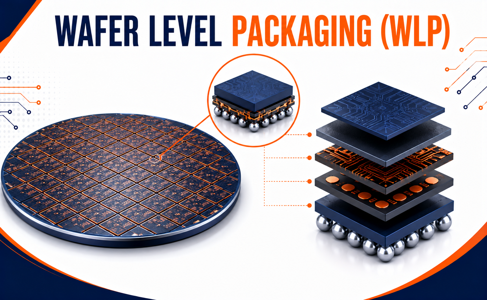
As semiconductor devices become smaller, faster, and more powerful, packaging technology has become just as important as transistor scaling. Conventional packaging processes typically package individual dies after wafer fabrication, but advanced applications increasingly require smaller footprints, shorter electrical paths, and higher interconnect density.
Wafer Level Packaging (WLP) addresses these requirements by performing most or all of the packaging processes while the semiconductor devices are still arranged on the wafer. Instead of packaging each die individually after singulation, WLP enables multiple devices to be processed simultaneously, reducing package size and improving manufacturing efficiency.
What is Wafer Level Packaging?
Wafer Level Packaging (WLP) is an advanced semiconductor packaging technology in which packaging and interconnection structures are fabricated directly at the wafer level before the wafer is diced into individual semiconductor packages.
Unlike conventional packaging, where the die is first separated and then packaged, WLP integrates structures such as redistribution layers, passivation, and external connections while the dies are still part of the wafer.
Why Wafer Level Packaging is Important
Modern electronic products demand compact components without sacrificing performance. WLP helps address these requirements by reducing package dimensions and shortening electrical interconnects.
Key advantages include:
- Smaller package footprint
- Reduced package height
- Shorter electrical paths
- Lower parasitic capacitance and inductance
- Improved electrical performance
- Higher interconnect density
- Reduced packaging material usage
- Potential cost advantages through wafer-level processing
Types and Applications of WLP
Wafer Level Packaging includes several approaches designed for different performance and integration requirements.
Fan-In WLP
In Fan-In WLP, the external connections remain within approximately the footprint of the semiconductor die. It is widely used for compact and cost-sensitive devices.
Fan-Out WLP
Fan-Out WLP extends the interconnection area beyond the original die footprint, providing more space for I/O connections and enabling higher integration density.
Embedded Wafer-Level Packaging
Some advanced approaches embed semiconductor dies within a reconstructed wafer or molding compound before RDL formation, enabling larger interconnection areas.
Major Applications
WLP is widely used in:
- Mobile processors
- Power management ICs
- RF components
- MEMS and sensors
- Image sensors
- Wearable electronics
- Automotive electronics
- Internet of Things (IoT) devices
The Future of Wafer Level Packaging
The continued growth of AI, edge computing, automotive electronics, 5G/6G communication, and advanced sensors is driving demand for smaller and more capable semiconductor packages.
Future developments in WLP are expected to focus on:
- Finer-pitch redistribution layers
- Advanced fan-out architectures
- Higher-density I/O integration
- Improved thermal management
- Hybrid bonding integration
- Integration with chiplet architectures
- Advanced heterogeneous integration
- Automated wafer-level inspection and process control
Conclusion
Wafer Level Packaging (WLP) has transformed semiconductor packaging by moving critical packaging operations directly to the wafer level. By reducing package size, shortening electrical connections, and enabling high-density interconnects, WLP provides an effective solution for today’s increasingly compact electronic devices.
From smartphones and wearables to automotive systems and advanced computing platforms, WLP continues to evolve alongside semiconductor technology. As devices demand higher performance within smaller form factors, wafer-level packaging will remain an important foundation for the next generation of semiconductor integration.
Share your question in comments or talk to our mentor team for batch guidance.
Ask the Admin Team
Drop your basic question in comments: eligibility, prerequisites, tools, fee range, and placement support.
Our team reviews and responds regularly.