

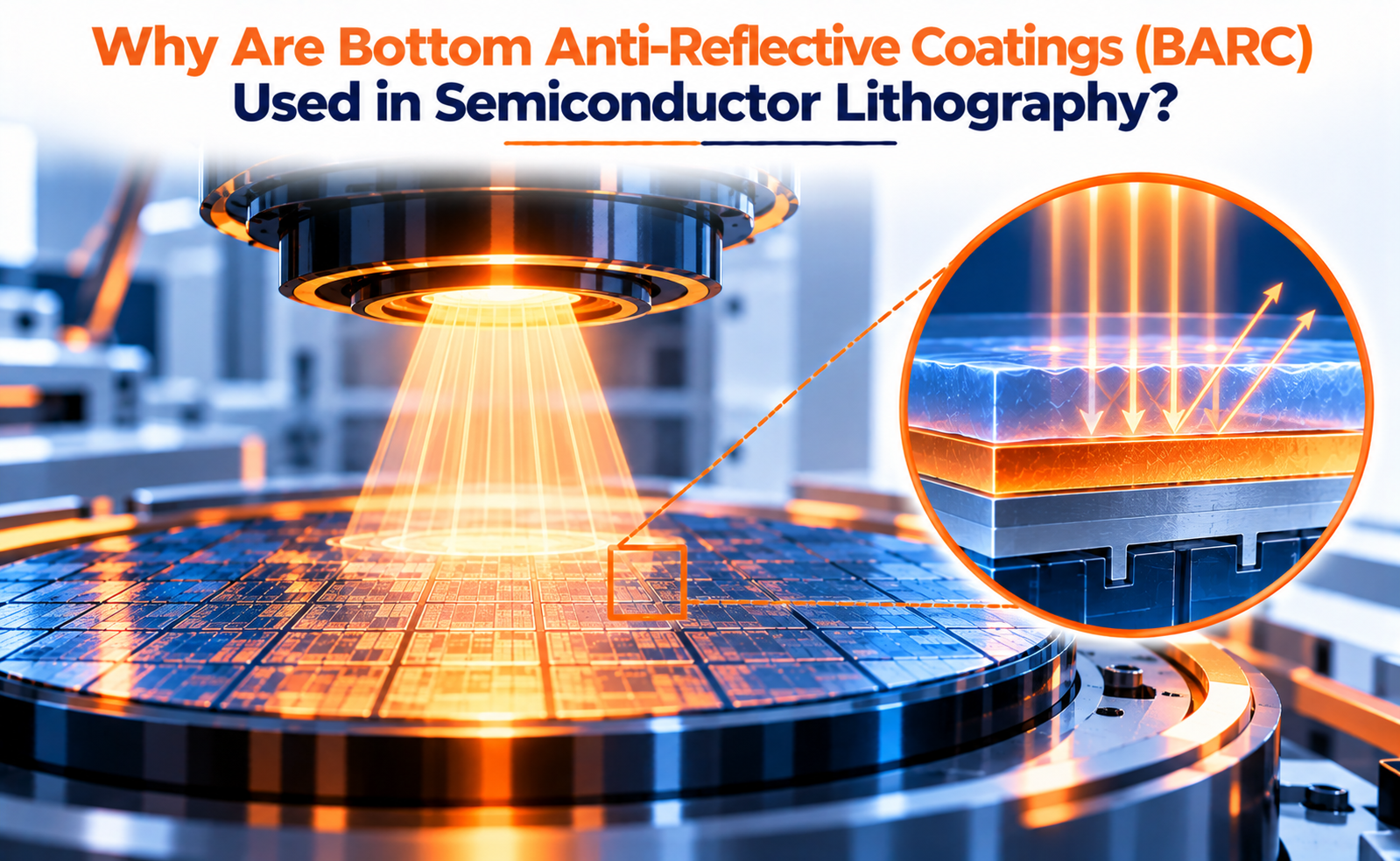
As semiconductor devices continue to shrink, lithography must reproduce increasingly smaller patterns with high precision. However, light used during photolithography can reflect from the underlying wafer layers and interfere with the exposure process. These reflections can distort the photoresist pattern, affect critical dimensions, and reduce manufacturing consistency.
Bottom Anti-Reflective Coatings (BARC) help address this challenge by reducing unwanted light reflections beneath the photoresist. By controlling reflected light, BARC improves lithographic pattern fidelity and supports the precise pattern transfer required in advanced semiconductor manufacturing.
What Is a Bottom Anti-Reflective Coating (BARC)?
A Bottom Anti-Reflective Coating is a thin material layer applied between the wafer surface and the photoresist during semiconductor photolithography.
During exposure, light passes through the photoresist and can reflect from the underlying films, such as dielectric layers, silicon, or metal structures. These reflected waves may interact with incoming light and produce unwanted variations in the exposure intensity.
BARC is designed to absorb or otherwise suppress these reflections before they return into the photoresist.
A simplified lithography stack is:
Exposure light → Photoresist → BARC → Underlying wafer layers
Depending on the application, BARC materials may be organic or inorganic. Organic BARC is commonly applied by spin coating, while inorganic anti-reflective layers may be deposited using techniques such as chemical vapor deposition.
The choice depends on the exposure wavelength, underlying materials, resist system, and integration requirements.
Why Is BARC Important in Semiconductor Lithography?
As lithographic dimensions decrease, small changes in exposure conditions can create significant patterning errors. Reflections from underlying layers can contribute to variations in photoresist exposure, especially when the underlying film stack has different optical properties or thicknesses.
BARC helps control these optical effects.
Key benefits include:
- Reduced reflective notching: Helps minimize distortions near patterned or reflective underlying features.
- Improved critical-dimension control: Reduces reflection-related variations in printed feature widths.
- Better pattern uniformity: Helps maintain more consistent lithographic patterns across different underlying structures.
- Improved process latitude: Reduces sensitivity to certain variations in the optical properties of underlying films.
- More reliable pattern transfer: Supports the formation of accurate patterns for subsequent etching and other fabrication steps.
BARC does not eliminate every lithography defect, but it helps reduce reflection-related sources of variation that can compromise pattern quality.
Challenges in BARC Selection and Process Control
Although BARC improves optical control, selecting and integrating the material requires careful engineering.
Thickness Uniformity
Variations in coating thickness can change the optical response across the wafer, potentially affecting lithographic uniformity.
Material Compatibility
BARC must be compatible with the photoresist, underlying films, and subsequent processing steps.
Etch Compatibility
The coating must be removable or patternable under the intended process conditions without damaging the underlying material.
Defect Control
Particles, coating defects, poor adhesion, or material contamination can create lithographic defects.
Optical Optimization
The ideal BARC formulation and thickness depend on the exposure wavelength, refractive indices, underlying stack, and patterning requirements. A solution optimized for one process may not perform equally well in another.
Advanced Lithography Requirements
As semiconductor manufacturing adopts advanced optical lithography and increasingly complex patterning techniques, reflection control must be integrated with other approaches for improving resolution and process stability.
BARC is therefore one component of a broader lithography optimization strategy that also includes photoresist engineering, exposure control, mask design, and etch integration.
The Future of BARC in Advanced Semiconductor Manufacturing
As semiconductor manufacturing moves toward smaller features and more complex material stacks, anti-reflective coating technology continues to evolve.
Future development is likely to focus on:
- Improved optical absorption at specific exposure wavelengths
- Better coating uniformity on complex wafer topography
- Compatibility with advanced photoresists
- Low-defect coating processes
- Improved etch selectivity
- Optimized materials for advanced lithography stacks
- Integration with next-generation patterning technologies
The growing complexity of semiconductor structures makes optical control increasingly important. BARC will continue to serve as a useful technique for reducing unwanted reflections wherever the lithography stack and process conditions require it.
Its effectiveness will depend on selecting the right material, controlling film thickness, and integrating the coating with the complete lithography and pattern-transfer process.
Conclusion
Bottom Anti-Reflective Coatings help improve semiconductor lithography by reducing unwanted light reflections from underlying wafer layers.
By controlling reflection-related exposure variations, BARC supports better critical-dimension control, pattern uniformity, and lithographic process stability.
Although it cannot eliminate every source of patterning error, BARC remains an important part of lithography stack engineering. As semiconductor features continue to shrink, careful optimization of anti-reflective coatings will help manufacturers maintain the precision required for advanced chip fabrication.
Share your question in comments or talk to our mentor team for batch guidance.
Ask the Admin Team
Drop your basic question in comments: eligibility, prerequisites, tools, fee range, and placement support.
Our team reviews and responds regularly.