

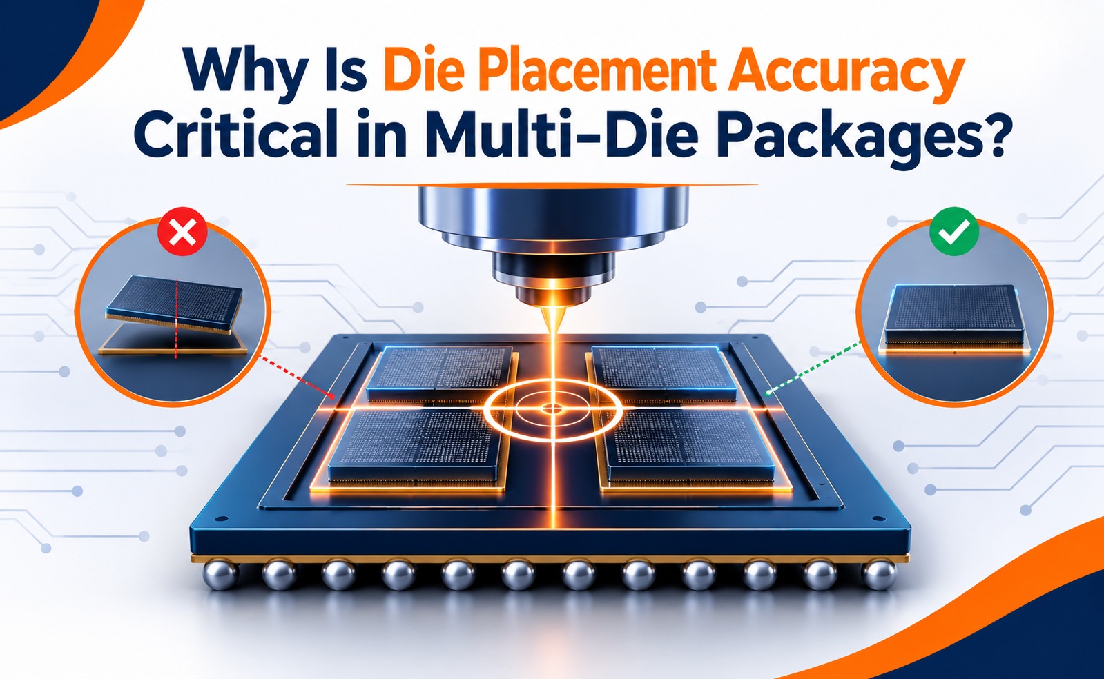
Die placement accuracy is a major requirement in advanced semiconductor packaging because multiple dies must be positioned precisely to establish reliable electrical and mechanical connections. In multi-die packages, even small placement errors can affect microbump alignment, interconnect reliability, signal integrity, thermal performance, and overall package yield.
As chiplet-based architectures and 2.5D and 3D integration become more common, precise die placement is essential for connecting processors, memory stacks, and specialized chiplets within a compact package.
What Is Die Placement Accuracy?
Die placement accuracy refers to how precisely a semiconductor die is positioned on a substrate, interposer, carrier wafer, or another die during package assembly.
The placement process must control three important alignment parameters:
- X-axis alignment: Controls horizontal positioning of the die.
- Y-axis alignment: Controls vertical positioning of the die.
- Theta alignment: Controls the rotational orientation of the die.
All three parameters are important because a die can be positioned correctly at its center but still have misaligned interconnects near its edges if its rotational orientation is incorrect.
In multi-die packaging, several dies must be positioned according to predefined layout coordinates to ensure that their electrical connections match the corresponding pads and interconnect structures.
Why Is Accurate Die Placement Important in Multi-Die Packages?
Multi-die packages integrate multiple semiconductor components within a single package to achieve higher performance, greater functionality, and improved integration flexibility.
These packages may contain:
- Logic dies and processor chiplets.
- High Bandwidth Memory (HBM) stacks.
- Input/output dies.
- Silicon interposers.
- Bridge dies.
- Redistribution layers (RDL).
- Through-Silicon Vias (TSVs).
Each component must connect through carefully designed electrical interfaces.
Accurate die placement helps achieve:
Reliable electrical connectivity: Ensures that corresponding bumps, pads, and interconnects align correctly.
High-density integration: Supports smaller interconnect pitches and more connections within limited package areas.
Signal integrity: Helps maintain the intended interconnect geometry and electrical characteristics.
Mechanical reliability: Reduces unwanted stress and uneven loading at bonding interfaces.
Higher manufacturing yield: Minimizes placement-related defects and electrical connection failures.
Without precise positioning, even properly fabricated dies may fail during package assembly.
How Does Die Misalignment Affect Electrical Connectivity?
One of the most important consequences of inaccurate die placement is electrical interconnect failure.
In advanced packages, dies are connected through dense arrays of microbumps, copper pads, TSVs, and redistribution-layer structures.
These connections require accurate alignment.
When a die shifts from its intended position, several problems can occur.
Open Connections: A bump or bonding pad may no longer overlap its corresponding connection point, resulting in an open electrical path.
Short Circuits: Misaligned conductive structures may approach neighboring connections and create unwanted electrical contact.
Increased Contact Resistance: Partial overlap between conductive interfaces can reduce the effective contact area and increase electrical resistance.
Interconnect Reliability Problems: Misalignment can create uneven bonding pressure and local mechanical stress.
Signal Transmission Issues: Changes in the intended interconnect geometry can affect electrical performance, particularly in high-speed die-to-die interfaces.
In fine-pitch hybrid bonding, placement and overlay accuracy become especially demanding because the bonding structures are extremely small.
What Is the Impact of Placement Accuracy on Microbumps and Hybrid Bonding?
Die placement accuracy becomes increasingly important as interconnect pitch decreases.
Microbump-Based Interconnects
Microbumps provide electrical and mechanical connections between dies and substrates or interposers.
During thermocompression bonding, the microbumps must align with their corresponding pads.
If the die is displaced, the overlap between the bumps and pads can decrease.
This may result in incomplete bonding, increased resistance, or open connections.
Hybrid Bonding
Hybrid bonding creates direct electrical and mechanical connections through aligned dielectric and metal surfaces, commonly copper-to-copper connections.
Unlike conventional solder-based approaches, hybrid bonding requires extremely precise surface alignment and excellent planarity.
Even small alignment errors can reduce copper-pad overlap or cause bonding defects.
Therefore, hybrid bonding requires much tighter placement and surface-control capabilities than many conventional assembly processes.
The required alignment tolerance depends on pad dimensions, pitch, bonding technology, and process design.
Why Is Die Placement Accuracy Important for Advanced Packaging Technologies?
Die placement accuracy is becoming increasingly important as semiconductor packages integrate more dies with smaller and denser electrical connections.
2.5D Packaging
In 2.5D packaging, multiple dies are mounted on a silicon interposer or another high-density routing structure.
Accurate placement is required to align die connections with interposer routing and microbump arrays.
3D IC Integration
In 3D integration, dies are stacked vertically to achieve higher integration density.
Placement accuracy is essential for aligning TSVs, bonding pads, and vertical interconnect structures.
Chiplet-Based Architecture
Chiplet packages integrate different functional dies, potentially manufactured using different process technologies.
Accurate positioning helps establish reliable die-to-die communication and maintain the intended package layout.
HBM Integration
HBM stacks are integrated alongside processors and AI accelerators using advanced packaging technologies.
Precise die placement is necessary to establish reliable high-density connections between memory and logic components.
As interconnect pitches become smaller, accurate placement and post-bond alignment control become increasingly important for package performance and yield.
Conclusion
Die placement accuracy is a fundamental requirement in multi-die semiconductor packaging because it directly influences electrical connectivity, bonding quality, mechanical reliability, and manufacturing yield.
Controlling X-axis, Y-axis, and rotational alignment helps ensure that microbumps, copper pads, TSVs, and other interconnect structures connect correctly.
However, accurate initial placement alone is not sufficient. Engineers must also control substrate warpage, thermal expansion, bonding conditions, and die movement during subsequent manufacturing operations.
As 2.5D integration, 3D stacking, HBM, and chiplet architectures continue to evolve, precision die placement will remain essential for building reliable, high-performance semiconductor packages.
Share your question in comments or talk to our mentor team for batch guidance.
Ask the Admin Team
Drop your basic question in comments: eligibility, prerequisites, tools, fee range, and placement support.
Our team reviews and responds regularly.