

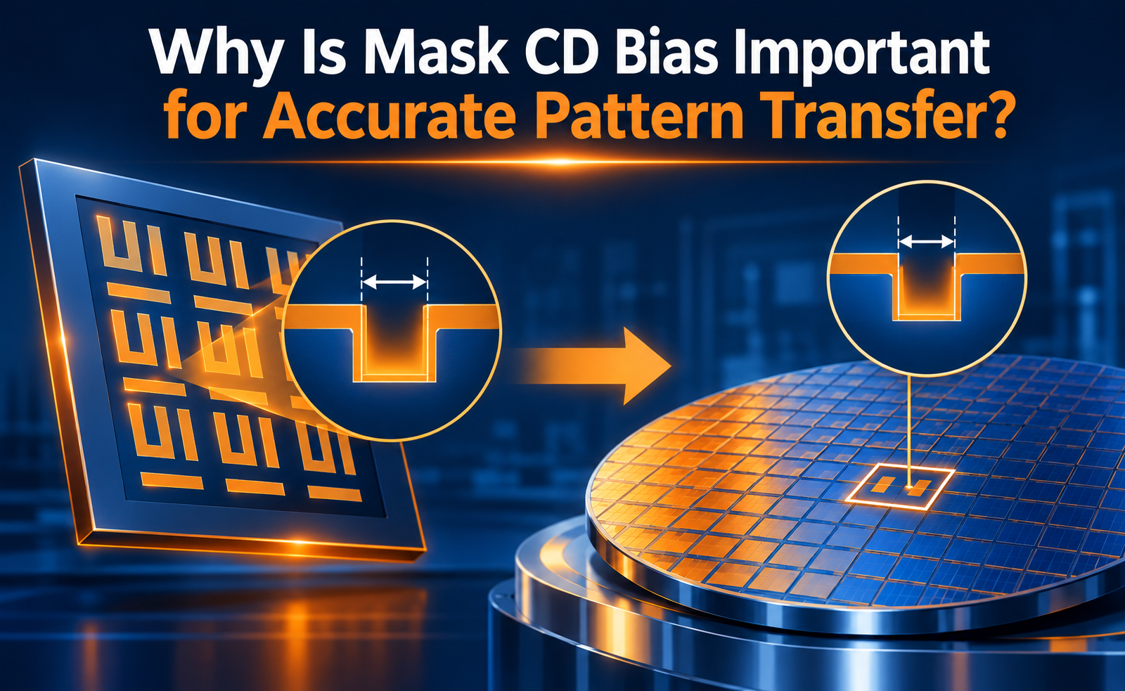
As semiconductor devices become smaller, controlling the dimensions of every patterned feature becomes increasingly important. During photolithography, a photomask transfers circuit patterns onto a photoresist-coated wafer using light. However, the dimensions printed on the wafer may differ from the original mask dimensions because of optical effects, resist behavior, and subsequent etching processes.
To compensate for these differences, semiconductor engineers use a technique called Mask Critical Dimension (CD) Biasing.
Mask CD bias involves intentionally adjusting the dimensions of features on a photomask so that the resulting wafer patterns match their intended design dimensions more accurately.
This technique is particularly important in advanced semiconductor manufacturing, where even small dimensional errors can affect transistor characteristics, circuit performance, and manufacturing yield.
What Is Mask CD Bias?
Critical Dimension (CD) refers to the measurement of an important feature in a semiconductor pattern, such as the width of a transistor gate, metal line, contact hole, or trench.
Mask CD bias is the intentional adjustment of photomask feature dimensions to compensate for dimensional changes during pattern transfer.
In a typical lithography process, the mask pattern is projected onto a wafer through an optical system. The projected image is then developed in photoresist and transferred into the underlying material through etching.
The final wafer feature may become wider or narrower than the dimension predicted by simply scaling the mask pattern.
Engineers therefore modify the mask dimensions to compensate for these effects.
For example:
- Target wafer feature width: 40 nm
- Lithography and process effects: feature prints approximately 4 nm narrower
- Required wafer-level correction: 4 nm
- Mask feature adjustment: increase the corresponding mask dimension, accounting for the exposure system’s reduction ratio
The actual correction is determined through process characterization and modeling rather than by applying a fixed value to every feature.
Why Is Mask CD Bias Required in Semiconductor Lithography?
A photomask does not transfer its pattern onto the wafer as a perfect geometric copy.
Several physical and process-related effects influence the final printed dimensions.
Optical diffraction: Light passing through or interacting with small mask features spreads and interferes, changing the aerial image formed on the wafer.
Optical proximity effects: Identical mask features can print differently depending on the spacing and arrangement of nearby structures.
Focus and exposure variations: Changes in focus and exposure dose can alter the dimensions of developed photoresist features.
Photoresist behavior: Resist thickness, chemical properties, exposure response, and development conditions influence the final resist CD.
Etch bias: During pattern transfer, lateral etching or sidewall profile changes can make the final etched feature wider or narrower than the photoresist pattern.
Because of these effects, engineers must determine how the complete lithography and etch process changes feature dimensions and compensate accordingly.
How Does Mask CD Bias Improve Optical Proximity Correction?
Optical Proximity Correction (OPC) is a lithography enhancement technique used to compensate for distortions introduced during optical pattern transfer.
At advanced technology nodes, optical effects can cause wafer patterns to differ significantly from the intended mask geometry.
For example:
- Line ends may become shorter than intended.
- Corners may become rounded.
- Isolated lines may print differently from dense lines.
- Closely spaced features may experience different dimensional changes.
Mask CD bias helps compensate for these variations by modifying feature dimensions.
In OPC, different corrections may be applied depending on the local pattern environment.
Common correction techniques include:
Global CD bias: Applies a general dimensional adjustment to a group of mask features.
Local CD bias: Applies different corrections to individual features based on their surroundings.
Serif correction: Adds small geometric features near corners to compensate for optical corner rounding.
Line-end correction: Extends or modifies line ends to compensate for line-end shortening.
Sub-Resolution Assist Features (SRAFs): Adds non-printing mask features that improve the aerial image of nearby functional patterns.
These corrections help produce more accurate wafer-level patterns.
What Happens When Mask CD Bias Is Incorrect?
Incorrect mask CD bias can introduce systematic dimensional errors across the wafer.
If the correction is too small, too large, or applied inconsistently, the final printed dimensions may deviate from their target values.
Some possible consequences include:
Incorrect transistor gate dimensions: Changes in gate length can affect threshold voltage, drive current, and leakage behavior.
Line-width variation: Incorrect metal dimensions can influence electrical resistance and interconnect performance.
Contact and via problems: Incorrect feature dimensions can affect contact formation, electrical connectivity, and resistance.
Spacing violations: Features may become too close together, increasing the risk of shorts or other patterning defects.
Reduced process window: A poorly optimized mask correction may cause features to exceed CD tolerances under small focus or exposure variations.
Lower manufacturing yield: Repeated dimensional errors can affect large numbers of dies produced using the same photomask.
Therefore, accurate bias determination is essential for maintaining dimensional consistency.
Why Is Mask CD Bias Important for Advanced Semiconductor Nodes?
As semiconductor technology moves toward smaller feature dimensions, patterning tolerances become increasingly demanding.
A dimensional error that may be acceptable for a larger feature can become significant for a much smaller transistor or interconnect structure.
Mask CD bias is important because it helps:
- Maintain accurate transistor gate dimensions.
- Improve critical feature uniformity.
- Compensate for optical proximity effects.
- Support accurate contact and via patterning.
- Improve consistency between mask design and wafer fabrication.
- Reduce systematic CD errors.
- Support advanced lithography processes, including EUV patterning.
At advanced technology nodes, mask corrections must also account for complex mask effects, resist behavior, stochastic variations, and process integration requirements.
Accurate mask CD bias therefore contributes to the overall dimensional control needed for high-performance semiconductor devices.
Conclusion
Mask CD bias is an essential technique for achieving accurate pattern transfer in semiconductor lithography.
Because optical diffraction, proximity effects, resist behavior, and etching can change feature dimensions, the mask pattern often requires intentional adjustments before exposure.
By combining CD measurements, lithography modeling, OPC, and process characterization, engineers determine the appropriate mask corrections to achieve the required wafer dimensions.
As semiconductor devices continue to scale, precise mask CD bias control remains important for transistor fabrication, interconnect patterning, process uniformity, and manufacturing yield.
Share your question in comments or talk to our mentor team for batch guidance.
Ask the Admin Team
Drop your basic question in comments: eligibility, prerequisites, tools, fee range, and placement support.
Our team reviews and responds regularly.