

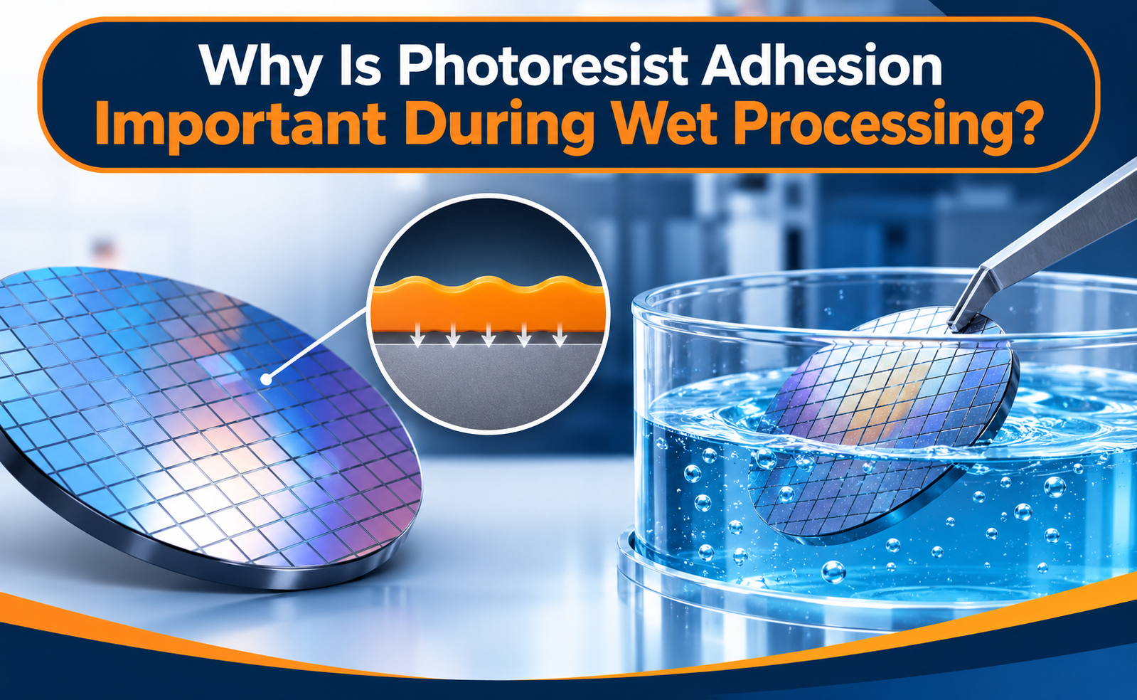
Photoresist adhesion is essential during semiconductor wet processing because the patterned resist must remain firmly attached to the wafer while exposed to chemical solutions, rinsing, and drying. Poor adhesion can cause resist lifting, peeling, pattern deformation, and unwanted chemical attack on areas that should remain protected.
Maintaining strong photoresist adhesion helps preserve pattern integrity, improve etch selectivity, and prevent defects that can reduce semiconductor manufacturing yield.
What Is Photoresist Adhesion?
Photoresist adhesion refers to the ability of a photoresist film to remain attached to the surface of a semiconductor wafer throughout lithography and subsequent processing.
During photolithography, a thin layer of photoresist is applied to the wafer using a spin-coating process. The resist is exposed to light through a photomask and developed to create the required pattern.
The remaining photoresist acts as a temporary protective layer during subsequent manufacturing operations.
For example, during wet etching, the exposed wafer regions are removed by chemical solutions, while the photoresist protects the regions that must remain unchanged.
If the resist does not adhere properly, chemicals can penetrate underneath the patterned layer and attack the protected material.
Therefore, good adhesion is necessary to maintain accurate pattern transfer throughout the manufacturing process.
Why Is Photoresist Adhesion Important During Wet Processing?
Wet processing involves exposing semiconductor wafers to liquid chemicals for cleaning, developing, etching, and other surface-treatment operations.
These processes can place stress on the photoresist-substrate interface.
Good adhesion is important for several reasons.
Pattern protection: The photoresist must remain attached to protect selected wafer regions from chemical attack.
Dimensional accuracy: Strong adhesion prevents patterned features from lifting, shifting, or deforming during chemical treatment.
Etch uniformity: Properly attached resist helps maintain consistent protection across the wafer surface.
Defect prevention: Good adhesion reduces peeling, delamination, undercutting, and unwanted material removal.
Manufacturing yield: Maintaining pattern integrity helps prevent defects that could make semiconductor devices electrically or physically unusable.
Without adequate adhesion, even a correctly patterned wafer can develop defects during subsequent wet processing.
What Factors Affect Photoresist Adhesion?
Several surface and process conditions influence how strongly photoresist attaches to a semiconductor wafer.
1. Surface Moisture
Moisture is one of the major causes of poor photoresist adhesion.
Silicon dioxide and other oxidized surfaces can retain water from the surrounding environment.
This moisture interferes with resist adhesion and can allow processing chemicals to penetrate the interface.
A dehydration bake is commonly used to remove adsorbed moisture before resist coating.
2. Surface Contamination
Organic residues, particles, and chemical contaminants can prevent uniform contact between the photoresist and the wafer.
Proper wafer cleaning is therefore essential before photoresist application.
3. Surface Energy and Wettability
The chemical nature of the wafer surface affects how the photoresist spreads and attaches.
Hydrophilic surfaces may exhibit poor compatibility with certain photoresist systems.
Surface conditioning can improve wettability and promote adhesion.
4. Photoresist Properties
Photoresist formulation, solvent composition, viscosity, and chemical compatibility influence the quality of the resist-substrate interface.
Different resist formulations may require different surface preparation and baking conditions.
5. Baking Conditions
Soft-bake conditions influence solvent removal and the physical properties of the photoresist film.
Insufficient or excessive baking can affect resist performance and adhesion.
6. Wet Chemical Conditions
Etchant composition, concentration, temperature, exposure duration, and liquid agitation can influence resist stability during wet processing.
The selected photoresist must be compatible with the intended chemical process.
How Does HMDS Improve Photoresist Adhesion?
Hexamethyldisilazane (HMDS) is a commonly used adhesion promoter in semiconductor photolithography.
It is applied to prepare suitable wafer surfaces before photoresist coating.
Oxidized silicon surfaces, such as silicon dioxide, are naturally hydrophilic and can retain moisture.
HMDS reacts with surface hydroxyl groups and replaces them with trimethylsilyl groups, making the surface more hydrophobic.
This surface modification helps reduce moisture-related adhesion problems and improves compatibility between the wafer surface and the organic photoresist.
The typical surface preparation sequence involves:
- Cleaning the wafer to remove particles and contaminants.
- Performing a dehydration bake to remove adsorbed moisture.
- Applying HMDS through an appropriate vapor or liquid priming process.
- Coating the wafer with photoresist.
- Performing a soft bake under controlled conditions.
The effectiveness of HMDS treatment can be evaluated using contact-angle measurements.
A properly prepared surface generally provides more reliable photoresist adhesion during development and subsequent wet processing.
What Defects Can Occur Due to Poor Photoresist Adhesion?
Poor photoresist adhesion can introduce several defects during semiconductor manufacturing.
Resist Peeling: Portions of the photoresist separate from the wafer surface, exposing areas that should remain protected.
Resist Lifting: Small patterned structures detach during development, rinsing, or chemical treatment.
Etch Undercutting: Wet etchants penetrate beneath the resist edges and remove material laterally from protected regions.
Pattern Distortion: The original pattern geometry changes because of partial resist detachment or chemical penetration.
Incomplete Surface Protection: Exposed regions receive unwanted chemical treatment, resulting in dimensional or material variations.
Particle Generation: Detached photoresist fragments can become contamination sources during wafer processing.
These defects can affect device dimensions, electrical characteristics, and overall manufacturing yield.
Why Is Photoresist Adhesion Important for Advanced Semiconductor Manufacturing?
Advanced semiconductor devices contain increasingly small structures, narrow interconnects, and complex material layers.
As dimensions shrink, even minor resist lifting or chemical penetration can cause significant patterning errors.
Photoresist adhesion is especially important in:
Advanced CMOS Fabrication: Protects patterned regions during selective material removal and surface preparation.
MEMS Manufacturing: Maintains accurate resist patterns during extended wet etching and structural release operations.
Interconnect Fabrication: Helps protect metal and dielectric regions during wet chemical processing.
Contact and Via Patterning: Maintains accurate openings and surrounding protective structures during material removal.
Wafer-Level Packaging: Supports reliable pattern protection during redistribution-layer fabrication and other wet chemical operations.
In these applications, strong adhesion contributes to dimensional accuracy, process consistency, and reliable device fabrication.
Conclusion
Photoresist adhesion is a critical requirement in semiconductor wet processing because the resist must remain firmly attached to the wafer while exposed to chemical solutions.
Poor adhesion can allow chemicals to penetrate beneath the resist, causing peeling, lifting, etch undercutting, and unwanted material removal.
Proper wafer cleaning, dehydration baking, HMDS priming, optimized resist processing, and controlled wet chemical conditions help maintain a reliable resist-substrate interface.
As semiconductor structures become smaller and manufacturing processes become more complex, effective photoresist adhesion control remains essential for accurate pattern transfer, defect reduction, and improved semiconductor manufacturing yield.
Share your question in comments or talk to our mentor team for batch guidance.
Ask the Admin Team
Drop your basic question in comments: eligibility, prerequisites, tools, fee range, and placement support.
Our team reviews and responds regularly.