

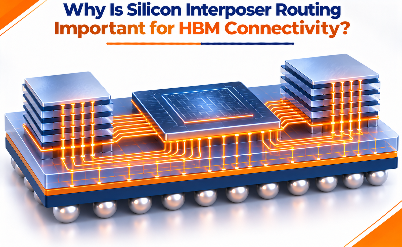
High Bandwidth Memory (HBM) is widely used in AI accelerators, GPUs, high-performance computing systems, and other applications that require extremely fast data access. Unlike conventional memory packages, HBM uses vertically stacked DRAM dies connected through Through-Silicon Vias (TSVs).
However, stacking memory dies alone is not enough. The HBM stack must also communicate with a processor or logic die at very high speeds. This requires thousands of closely spaced electrical connections within a limited package area.
Silicon interposer routing plays a critical role in making this communication possible. A silicon interposer provides fine-pitch, multilayer wiring that connects HBM stacks to logic dies, enabling high-density signal transmission, efficient power distribution, and compact 2.5D integration.
What Is a Silicon Interposer?
A silicon interposer is a thin silicon-based structure placed between semiconductor dies and the package substrate.
It acts as an intermediate routing platform that electrically connects multiple dies within an advanced semiconductor package.
Unlike a conventional organic package substrate, a silicon interposer can support much finer wiring dimensions and smaller connection pitches.
Its main components include:
- Redistribution Layers (RDL): Fine metal wiring layers that route electrical signals between different dies.
- Through-Silicon Vias (TSVs): Vertical conductive connections that pass through the silicon interposer.
- Microbumps: Small conductive connections that electrically and mechanically connect the HBM and logic dies to the interposer.
- Dielectric Layers: Insulating materials that separate conductive routing layers.
- Power and Ground Networks: Conductive structures that distribute supply voltage and provide return-current paths.
Together, these components create a high-density interconnect platform for advanced packaging.
Why Does HBM Need Silicon Interposer Routing?
HBM is designed to transfer large amounts of data between memory and processing units.
To achieve this, HBM uses a very wide interface with numerous parallel data, command, address, clock, power, and ground connections.
Connecting all these signals through a conventional package substrate would be difficult because its routing pitch is generally much coarser than the fine-pitch connections required at the die level.
Silicon interposer routing addresses this challenge through:
High routing density: Fine-pitch metal wiring supports a large number of connections within a limited area.
Short interconnect paths: HBM and the processor can be placed close together, reducing the distance signals must travel.
Multilayer connectivity: Multiple metal layers allow signals, power, and ground connections to be distributed across the package.
Improved electrical performance: Carefully designed routing helps manage signal loss, reflections, crosstalk, and timing differences.
Compact integration: Multiple HBM stacks and logic dies can be integrated into a single advanced package.
These capabilities make silicon interposers particularly useful for high-bandwidth memory systems.
Why Is Routing Density Important for HBM Connectivity?
One of the most important requirements of HBM is its extremely wide interface.
For example, HBM3E uses a 1024-bit interface, while HBM4 expands the interface to 2048 bits.
A wider interface enables more data to be transferred in parallel, but it also increases the number of physical connections that must be routed.
The interposer must accommodate:
- Thousands of fine-pitch signal connections.
- Data and command routing between HBM and logic dies.
- Clock distribution networks.
- Power and ground connections.
- Test and monitoring signals.
- Routing escape paths around microbump arrays.
Without sufficient routing density, it becomes difficult to connect all these signals within the available package area.
Silicon interposers provide the fine wiring pitch and multilayer routing capability needed to manage this complexity.
How Does Interposer Routing Affect Signal Integrity?
HBM interfaces operate at high data rates and use a large number of parallel electrical signals.
As routing density increases, signal integrity becomes an important design consideration.
Several electrical effects must be controlled.
Crosstalk: Closely spaced signal traces can couple electromagnetic energy into neighboring traces, potentially disturbing transmitted data.
Signal Loss: Resistance and dielectric losses along interconnect paths can reduce signal amplitude.
Impedance Discontinuities: Changes in trace geometry, vias, bumps, and transitions can create reflections.
Timing Skew: Differences in signal path lengths can cause data signals to arrive at different times.
Jitter: Noise and timing variations can affect the accuracy of signal transitions.
To manage these issues, engineers use careful routing strategies such as:
- Controlled trace spacing.
- Ground shielding and reference structures.
- Appropriate signal-layer assignment.
- Length matching where required.
- Optimized via and microbump transitions.
- Signal-integrity simulation and post-layout verification.
These techniques help maintain reliable high-speed communication between HBM and the processor.
Why Are Power and Ground Routing Important?
HBM and high-performance processors require stable power delivery during operation.
Large numbers of signals may switch simultaneously, creating substantial current demand and electrical noise.
The silicon interposer must therefore support both signal routing and power distribution.
Power and ground routing helps:
Reduce IR drop: Adequate conductive paths help minimize voltage loss caused by resistance.
Control ground bounce: Proper return paths help reduce unwanted ground-voltage fluctuations.
Reduce simultaneous switching noise: Carefully designed power and ground networks help manage noise generated by many switching signals.
Improve supply stability: A well-designed power distribution network helps maintain stable voltage at the connected dies.
Power integrity must be considered alongside signal integrity because poor supply conditions can affect data transmission and overall system reliability.
What Are the Challenges in Silicon Interposer Routing?
Although silicon interposers provide high routing density, designing and manufacturing them introduces several challenges.
1. Routing Congestion
The large number of HBM connections creates high routing demand around die edges and microbump arrays.
Engineers must carefully plan signal escape routes and metal-layer allocation.
2. Crosstalk and Signal Coupling
Closely spaced metal traces can produce unwanted coupling.
Routing patterns, shielding, and detailed electromagnetic analysis are needed to control these effects.
3. TSV Placement Constraints
TSVs require dedicated space and may introduce keep-out regions that affect nearby routing.
Their placement must be coordinated with signal paths, power networks, and mechanical requirements.
4. Power Distribution Complexity
The interposer must distribute sufficient power to the HBM and logic dies while controlling voltage drop and supply noise.
5. Manufacturing Cost
Fine-pitch redistribution layers, TSV fabrication, wafer thinning, and precision assembly increase manufacturing complexity and cost.
6. Thermal and Mechanical Reliability
The processor and HBM stacks generate heat during operation. Differences in material properties and temperature distribution can create mechanical stress, warpage, and reliability concerns.
These challenges require coordinated chip, interposer, and package design.
Where Is Silicon Interposer Routing Used?
Silicon interposer routing is especially important in advanced semiconductor packages that integrate high-bandwidth memory with processing devices.
Common applications include:
AI Accelerators: Connects multiple HBM stacks to compute dies that process large AI workloads.
Graphics Processing Units (GPUs): Enables high-speed communication between graphics processors and HBM.
High-Performance Computing: Supports memory-intensive workloads that require high data-transfer bandwidth.
Networking and Data Center Processors: Helps integrate high-performance logic and memory within compact packages.
Advanced 2.5D Packaging: Supports heterogeneous integration of multiple dies, including processors, chiplets, and memory stacks.
Technologies such as TSMC’s CoWoS-S are examples of advanced packaging approaches that use silicon interposers for high-density die-to-die connectivity.
Conclusion
Silicon interposer routing is a critical part of HBM connectivity because it provides the fine-pitch, high-density electrical connections required between memory stacks and high-performance logic dies.
By combining multilayer redistribution wiring, TSVs, and microbump connections, the interposer enables wide parallel interfaces within a compact package.
However, achieving reliable HBM connectivity requires more than simply connecting the dies. Engineers must carefully optimize routing density, signal integrity, power delivery, thermal behavior, and manufacturing constraints.
As HBM interfaces become wider and data rates increase, silicon interposer routing will remain an important technology for advanced packaging used in AI accelerators, GPUs, and high-performance computing systems.
Share your question in comments or talk to our mentor team for batch guidance.
Ask the Admin Team
Drop your basic question in comments: eligibility, prerequisites, tools, fee range, and placement support.
Our team reviews and responds regularly.