

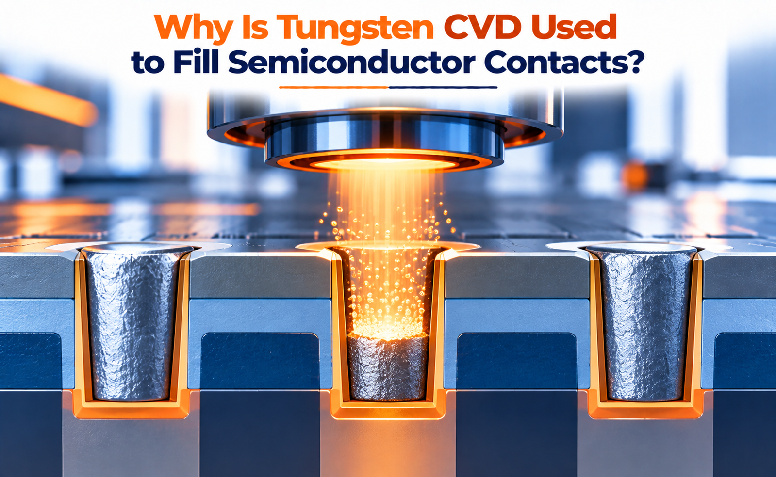
As semiconductor devices continue to shrink, connecting transistors to the metal interconnect network becomes increasingly challenging. Semiconductor contacts must provide reliable electrical connections through narrow, high-aspect-ratio openings while maintaining low resistance and compatibility with surrounding materials.
Tungsten Chemical Vapor Deposition (W CVD) is an established technology used to fill many semiconductor contact structures. Its ability to deposit tungsten inside narrow openings, combined with its relatively high melting point and compatibility with established contact integration processes, makes it valuable in front-end and middle-of-line manufacturing.
From transistor contacts to contact plugs in complex integrated circuits, tungsten CVD helps create the vertical electrical connections needed to link semiconductor devices with higher-level interconnects.
What Is Tungsten CVD in Semiconductor Manufacturing?
Tungsten CVD is a deposition process that forms a solid tungsten film through chemical reactions involving gaseous precursors at the wafer surface.
In semiconductor manufacturing, tungsten is commonly deposited into contact holes or vias that have been etched into dielectric materials. These openings connect transistor terminals or other device regions to the interconnect structure.
A simplified contact structure contains:
- Silicon or another underlying conductive region
- A contact interface or liner, depending on the integration scheme
- A barrier or nucleation layer, where required
- A tungsten-filled contact plug
- An overlying metal interconnect
The tungsten fills the opening to create a conductive pathway through the dielectric.
Unlike a simple line-of-sight deposition process, CVD relies on chemical reactions at accessible surfaces. This makes it suitable for filling contact openings with relatively high aspect ratios, provided the process conditions are optimized to avoid seams and voids.
Why Is Tungsten Preferred for Contact Filling?
Tungsten offers a combination of material and process characteristics that makes it useful for semiconductor contacts.
Good Filling Capability
CVD tungsten can deposit material within narrow contact openings and can be optimized for high-aspect-ratio structures.
High Thermal Stability
Tungsten has a high melting point and strong thermal stability, making it suitable for many semiconductor process environments.
Established Process Integration
Tungsten contact formation has a long history in semiconductor manufacturing. Mature deposition, etch-back, and planarization approaches support its integration into established process flows.
Useful Electrical Conductivity
Tungsten provides a conductive pathway between the underlying device region and the interconnect system.
However, tungsten does not automatically provide the lowest possible contact resistance. At very small dimensions, the resistivity of the deposited film, contact interface resistance, liner thickness, and contact geometry all affect the final electrical performance.
Compatibility With Contact Structures
Tungsten can be integrated with suitable liners and interface materials to help manage adhesion, nucleation, and unwanted material interactions.
These combined advantages explain why tungsten remains an important contact-fill material, even as advanced semiconductor processes investigate alternative metals.
Key Benefits of Tungsten CVD
Tungsten CVD offers several benefits for contact formation.
industry-standard lint and equivalence tools deposition: Properly optimized CVD conditions can provide useful coverage inside narrow openings.
High-aspect-ratio filling: Tungsten deposition can be engineered for contact geometries that are difficult to fill using simpler deposition methods.
Process maturity: Established equipment, precursor delivery, and process-control techniques support reliable manufacturing.
Thermal robustness: Tungsten withstands high temperatures relative to many other conductive materials.
Integration flexibility: Tungsten plugs can be combined with suitable liners, contact-interface treatments, and downstream metal interconnect processes.
These advantages make tungsten CVD particularly useful where reliable vertical connections are required between transistor-level structures and the wider interconnect network.
The Future of Tungsten Contact Technology
Tungsten CVD remains important in semiconductor manufacturing, but contact technology continues to evolve as transistor architectures and device dimensions change.
Future development is likely to focus on:
- Improved tungsten nucleation
- Better seam-free and void-free filling
- Reduced contact resistance
- Thinner and more efficient liner structures
- Improved control of fluorine-related interactions
- Advanced precursor and deposition chemistry
- Better integration with scaled transistor contacts
- Evaluation of alternative conductive materials for selected applications
At the same time, advanced device architectures—including FinFETs and gate-all-around transistors—place increasing demands on contact resistance and dimensional control.
The best contact material therefore depends on the device architecture, contact geometry, process thermal budget, electrical requirements, and manufacturing integration. Tungsten remains valuable where its deposition characteristics and established process flow provide a suitable solution.
Conclusion
Tungsten CVD is used to fill semiconductor contacts because it provides a mature and adaptable method for forming conductive plugs inside narrow contact openings.
Its deposition capability, thermal stability, electrical conductivity, and established integration methods make it an important technology for connecting transistor-level structures to semiconductor interconnects.
However, successful contact formation depends on more than filling the opening. Nucleation, liners, contact-interface resistance, void control, and material compatibility all influence final performance.
As semiconductor devices continue to scale, tungsten CVD will remain an important contact-fill technology while evolving alongside new materials, deposition methods, and advanced transistor architectures.
Share your question in comments or talk to our mentor team for batch guidance.
Ask the Admin Team
Drop your basic question in comments: eligibility, prerequisites, tools, fee range, and placement support.
Our team reviews and responds regularly.